
Diffusion process of low-pressure diffusion matching laser SE

A diffusion process and laser technology, applied in the field of solar cells, can solve the problems of poor diffusion process quality, aggravating the gap between silicon wafer doping concentration and edge, reducing photoelectric conversion efficiency and electrical performance yield and so on.

Active Publication Date: 2021-06-11
HUNAN RED SUN PHOTOELECTRICITY SCI & TECH
View PDF6 Cites 0 Cited by
  • Summary
  • Abstract
  • Description
  • Claims
  • Application Information

AI Technical Summary

Problems solved by technology

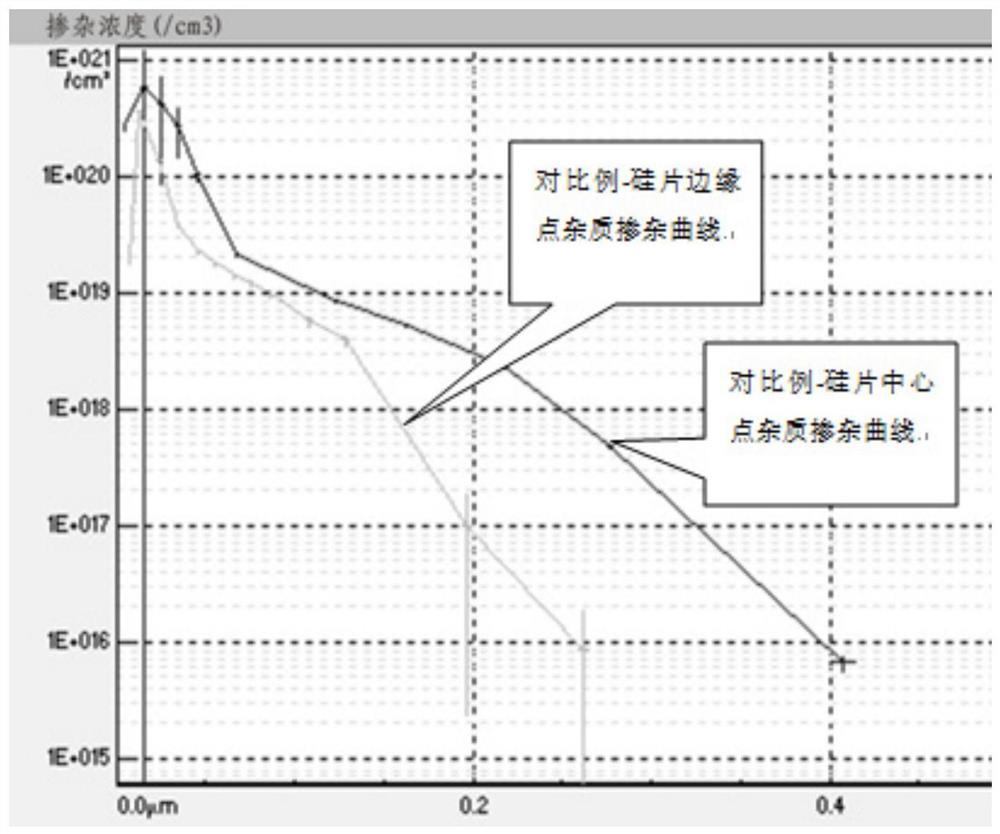
[0006] In order to reduce the doping amount of the diffused impurity source - phosphorus oxychloride, the current process parameter adjustment mainly reduces the concentration of the diffused impurity source, or reduces the low-temperature diffusion time of the diffused impurity source, and the adoption of this process method directly leads to the diffusion of doped atomic components. The pressure ratio is small, and the low impurity source concentration exacerbates the gap between the doping concentration in the middle of the silicon wafer and the edge, and the silicon wafer in the quartz boat has a more obvious concentration difference between the inlet area and the exhaust position in the furnace tube, and the quality of the diffusion process is poor. The uniformity of diffusion resistance is far from meeting the requirements of current technology
After the same silicon wafer is diffused, the impurity surface concentration and PN junction depth distribution are uniform, which not only affects the electrical properties of crystalline silicon solar cells, but also easily leads to the high temperature sintering process of the PN junction of monocrystalline silicon solar cells after screen printing, PN ending Partial burn-through; local square resistance of monocrystalline silicon solar cells is too high EL test black clusters, greatly reducing photoelectric conversion efficiency and electrical performance yield
[0007] To achieve high square resistance, if the doping concentration and the total amount of doping are not reduced on the basis of the normal diffusion square resistance process, it will directly lead to low square resistance. As a result, the surface concentration is too high, and the conversion efficiency of the battery is greatly reduced; if the subsequent high-temperature advance time is increased, although the surface concentration is reduced, the diffusion junction depth is increased, which will also reduce the short-wave spectral response of the battery and reduce the battery efficiency. At the same time, the process time is increased. Reduce production capacity
[0008] However, by reducing the low-temperature diffusion time of the impurity source and increasing the concentration of the impurity source to achieve the same total amount of the impurity source, this method makes it more difficult to control the uniformity of the diffusion square resistance due to the shortened diffusion time, and the uniformity of the square resistance within the chip is even worse.
[0009] The method of increasing the constant temperature time before the low-temperature diffusion of the diffusion impurity source to achieve a more balanced diffusion temperature of the low-temperature impurity source in the tube and the chip, although it can also improve the uniformity of the diffusion square resistance to a certain extent, but the improvement is very limited, and at the same time Increasing the constant temperature time will directly affect the production capacity
[0010] In addition, in the conventional diffusion process, the concentration of the diffusion source used is lower than 50%, and the diffusion resistance is uniform. Poor, the actual production process uniformity can not reach below 6%

Method used


Image

  • Diffusion process of low-pressure diffusion matching laser SE
  • Diffusion process of low-pressure diffusion matching laser SE
  • Diffusion process of low-pressure diffusion matching laser SE

Examples


Embodiment 1

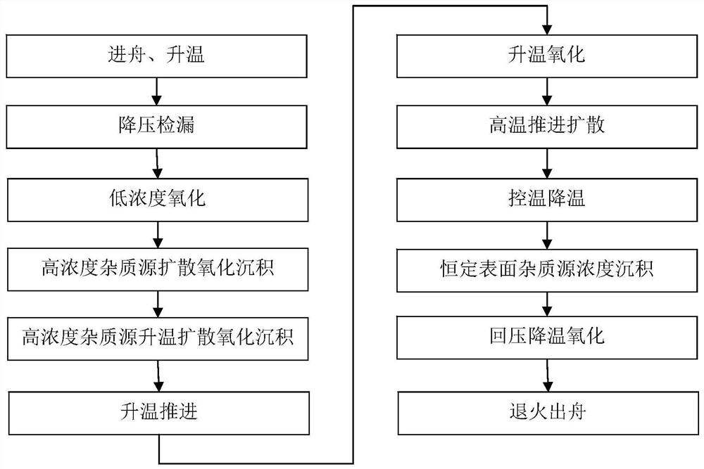
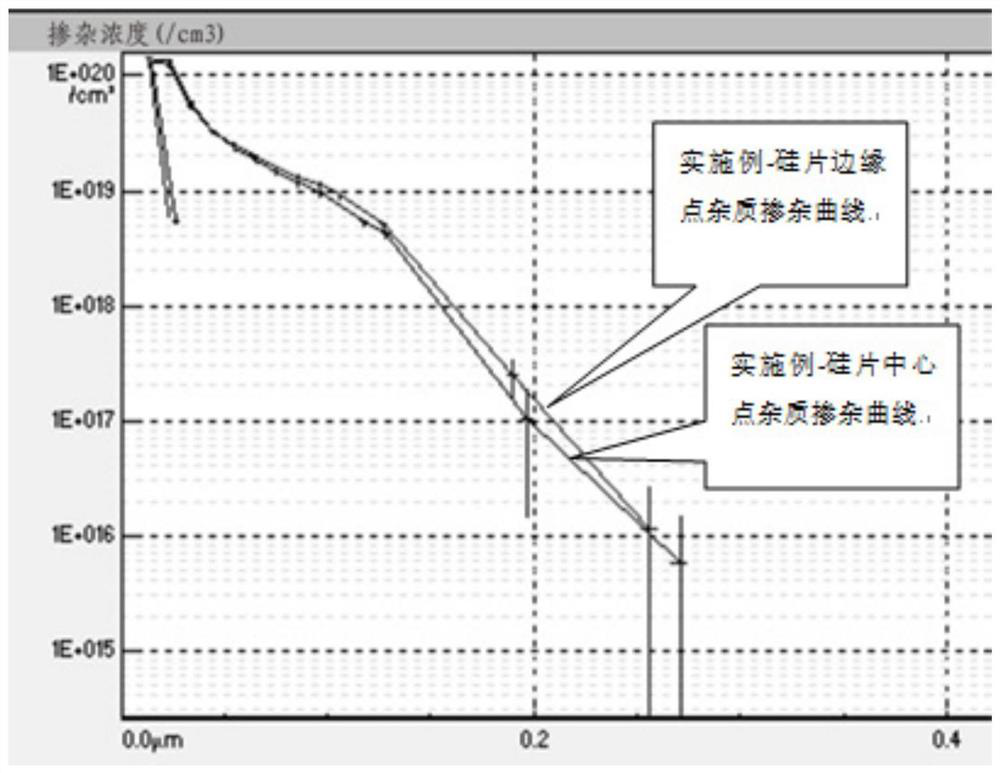
[0050] A low-voltage diffusion matching laser SE diffusion process, the diffusion process of the three groups of embodiment numbers of numbers SY001-003, such as figure 1 shown, including the following steps:

[0051] (1) Entering the boat and heating up: Insert the cleaned silicon wafer into the quartz boat and send it into the furnace tube of the diffusion equipment. During this process, nitrogen protection is introduced to preheat and heat up. The temperature is controlled to rise to 760 ° C ~ 800 ° C °C, the corresponding diffusion parameters of each example number refer to the following table 1-1.

[0052] Table 1-1 Process parameters corresponding to different numbers of diffusion processes

[0053]

[0054] (2) Step-down leak detection: start the vacuum pump, pump the pressure from normal pressure to low-pressure vacuum, and perform a leak detection test, wherein the pressure control is less than or equal to 100mbar, and the leak rate requirement is <2mbar / min; the ...


PUM

PropertyMeasurementUnit
Resistivityaaaaaaaaaa
Thicknessaaaaaaaaaa
Square resistanceaaaaaaaaaa

Abstract

The invention discloses a diffusion process of low-pressure diffusion matching laser SE. The diffusion process comprises the following steps of: carrying out low-concentration oxidation; conducting high-concentration impurity source diffusion, oxidation and deposition, so that the total quantity of impurity sources on the surface of a silicon wafer is greater than the total quantity of the impurity sources required by PN junction depth; performing high-concentration impurity source heating, diffusion, oxidation and deposition, so that the total quantity of the impurity sources on the surface of the silicon wafer is greater than the total quantity of the impurity sources required by PN junction depth; raising the temperature to advance; and carrying out heating oxidation, and carrying out rapid enhanced oxidation on the impurity sources until the total quantity of the impurity sources on the surface of the silicon wafer is the same as the total quantity of the impurity sources required by the PN junction depth. According to the diffusion process for the low-pressure diffusion matching laser SE, on the premise of not influencing the production capacity, the consistency of PN junction depth and the uniformity and stability of diffusion sheet resistance are improved, the cell conversion efficiency is improved, the use value is high, and the application prospect is good.

Description

technical field [0001] The invention belongs to the field of solar cells and relates to a low-voltage diffusion matching laser SE diffusion process. Background technique [0002] With the continuous development of PERC battery (Passivated Emitter and Rear Cell) full name passivated emitter and back local contact battery technology, the PERC technology that uses laser doping to form SE (Selective Emitter) full name selective emitter electrode has emerged as the times require. And has become the current mainstream technology. [0003] SE (Selective Emitter) selective emitter electrode, that is, high-concentration doping is performed on the front metallization gate line of the crystalline silicon cell and the contact area of ​​the silicon wafer to form a good ohmic contact and reduce the contact resistance between the metallization and the silicon wafer. Low-concentration doping in the non-contact area outside the electrodes improves the short-wave response of the battery, fur...

Claims


Application Information

Patent Timeline
IPC IPC(8): H01L31/18H01L21/225H01L31/068
CPCH01L31/1804H01L21/2252H01L21/2256H01L31/068Y02E10/547Y02P70/50
Inventor 邹臻峰李明赵增超任鹏石书清柳一峰黄心沿
Owner HUNAN RED SUN PHOTOELECTRICITY SCI & TECH
Learn More