IGBT chip and preparation method thereof

A technology of chip and conductive type, applied in the field of IGBT chip and its preparation, can solve the problems of large error, achieve the effect of low additional cost, improve performance and reliability, and expand the scope of application

Active Publication Date: 2021-06-25
ZHUZHOU CRRC TIMES SEMICON CO LTD
View PDF0 Cites 3 Cited by
  • Summary
  • Abstract
  • Description
  • Claims
  • Application Information

AI Technical Summary

Problems solved by technology

In order to prevent the IGBT from high temperature thermal failure, the temperature sensor is generally packaged inside the power module during the module packaging process, but the t

Method used


Image

  • IGBT chip and preparation method thereof
  • IGBT chip and preparation method thereof
  • IGBT chip and preparation method thereof

Examples


Embodiment 1

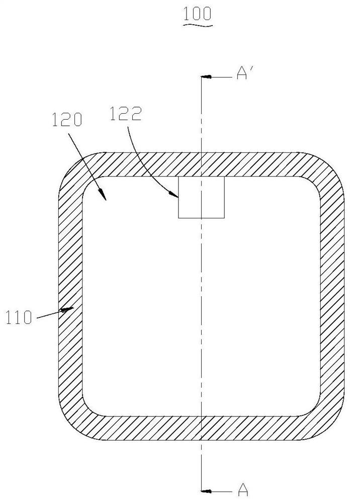
[0060] Such as figure 1 As shown, an IGBT chip 100 with a planar gate structure includes a terminal protection region 110 and a cell region 120 . The cell area 120 is located in the middle of the IGBT chip 100 , and the terminal protection area 110 is located at the edge of the IGBT chip 100 and surrounds the cell area 120 .

[0061] The cell area 120 includes an IGBT cell area 121 and a temperature sensing area 122 . The temperature sensing area 122 can be located at any position of the cellular area 120 , and in this embodiment, the temperature sensing area 122 is located at the edge of the cellular area 120 as an example.

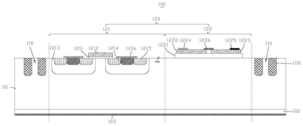
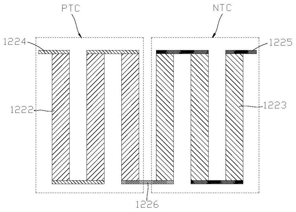
[0062] Such as figure 2 As shown, both the terminal protection region 110 and the cell region 120 include the substrate 101 of the IGBT chip, the collector layer 102 and the collector metal layer 103 .

[0063] Exemplarily, the substrate 101 is a substrate of the first conductivity type. The collector layer 102 is a collector layer of the second con...

Embodiment 2

[0103] Such as Figure 6 , an IGBT chip 200 with a planar gate structure, including a terminal protection region 210 and a cell region 220 . The cell area 220 includes an IGBT cell area 221 and a temperature sensing area 222 . The temperature sensing area 222 can be located at any position of the cellular area 220 , and in this embodiment, the temperature sensing area 222 is located at the edge of the cellular area 220 as an example.

[0104] Both the terminal protection area 210 and the cell area 220 include the substrate 201 of the IGBT chip, the collector layer 202 and the collector metal layer 203 .

[0105] Exemplarily, the substrate 201 is a substrate of the first conductivity type. The collector layer 202 is a collector layer of the second conductivity type and is located below the substrate 201 . The collector metal layer 203 is located under the collector layer 202 and forms an ohmic contact with the collector layer 202 .

[0106] The terminal protection area 210 ...

Embodiment 3

[0145] Such as Figure 9 As shown, on the basis of the first embodiment, this embodiment provides an IGBT chip 300 with a trench gate structure, which includes a terminal protection region 310 and a cell region 320 . The cell area 320 is located in the middle of the IGBT chip 300 , and the terminal protection area 310 is located at the edge of the IGBT chip 300 and surrounds the cell area 320 .

[0146] The cell area 320 includes an IGBT cell area 321 and a temperature sensing area 322 . The temperature sensing region 322 can be located at any position of the cellular region 320 , and in this embodiment, the temperature sensing region 322 is located at the edge of the cellular region 320 as an example.

[0147] Both the terminal protection area 310 and the cell area 320 include the substrate 101 of the IGBT chip, the collector layer 302 and the collector metal layer 303 .

[0148] Exemplarily, the substrate 101 is a substrate of the first conductivity type. The collector la...


PUM


Abstract

The invention provides an IGBT chip and a preparation method thereof. The IGBT chip comprises a terminal protection area and a cellular area, wherein the cellular area comprises an IGBT cell and a temperature sensing area, the temperature sensing area comprises a first conductive type substrate, a field oxide layer located above the substrate, a first polycrystalline silicon layer and a second polycrystalline silicon layer which are arranged side by side above the field oxide layer, and a first electrode, a second electrode and a third electrode which are located above the first polycrystalline silicon layer and the second polycrystalline silicon layer and are isolated from each other, wherein the first polycrystalline silicon layer is used for forming a positive temperature coefficient thermistor, and the second polycrystalline silicon layer is used for forming a negative temperature coefficient thermistor. According to the IGBT chip, a positive temperature coefficient thermistor (PTC) and a negative temperature coefficient thermistor (NTC) are integrated in an IGBT cellular area, and the NTC and the PTC resistor are connected in series to amplify an electrical signal generated by temperature change, so that the temperature detection sensitivity is improved so as to further improve the performance and the reliability of the IGBT chip.

Description

technical field [0001] The present disclosure relates to the technical field of semiconductor devices, in particular to an IGBT chip and a preparation method thereof. Background technique [0002] Insulated Gate Bipolar Transistor (IGBT) is a composite full-control voltage-driven power semiconductor device composed of BJT (bipolar transistor) and MOSFET (metal oxide semiconductor field effect transistor). The widest range of semiconductor devices in high voltage, high current, high frequency power electronics applications. [0003] The intelligent power module (IPM) is a switching device that encapsulates the sensing element, protection circuit and driving circuit inside the module. This device can improve the performance and reliability of the IGBT module and reduce the module volume. However, since the IGBT is a high-power semiconductor device, the large power loss makes the heating phenomenon serious. If the IGBT temperature is too high, it will affect the operation of t...

Claims


Application Information

Patent Timeline
IPC IPC(8): H01L29/739H01L21/335H01L29/06
CPCH01L29/7393H01L29/66325H01L29/0603H01L29/0684
Inventor 李迪宁旭斌肖强覃荣震
Owner ZHUZHOU CRRC TIMES SEMICON CO LTD
Why Eureka
Try Eureka