Palladium activation method for electro-less nickel immersion gold of PCB (printed circuit board)
A PCB circuit board and chemical nickel-gold technology, which is applied in the field of palladium activation of chemical nickel-gold on PCB circuit boards, can solve the problems of surface roughness, increase bonding ability, etc., achieve excellent soldering performance, eliminate false soldering, and be easy to process and use
- Summary
- Abstract
- Description
- Claims
- Application Information
AI Technical Summary
Problems solved by technology
Method used
Image

Examples
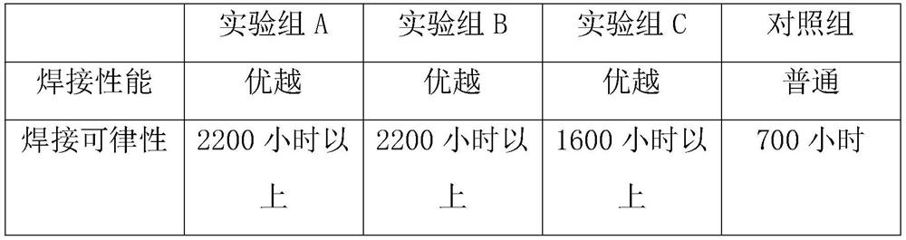
Embodiment 1
[0046] Step 1: Place the product in an acidic cleaner for degreasing cleaning;
[0047] Step 2: pickling with pickling solution, the pickling solution contains substances with a concentration of 5% retarder, remove surface oxides, use pickling solution to wash and remove acid again, after hydrogen displacement treatment, heat and dry at 200°C Bake for 4 hours, wash with water and put into the electroless palladium plating tank, and electroless palladium plating for 10 minutes;
[0048] Step 3: Put the product in hot water at 50°C for cleaning, then put it in ionized water for 1-3 minutes, and drain the cleaning water;
[0049] Step 4: Microetching the product to form a microstructure;
[0050] Step 5: put in ionized water and circulate for 1 minute, then drain the cleaning water;
[0051] Step 6: After putting the product into the phosphoric acid solution for 0.5 min, transfer it to an activation tank with a palladium activator, treat it at 25°C for 1 min, and deposit activa...
Embodiment 2
[0056] Step is the same as embodiment 1;
[0057] Step 2: pickling with pickling solution, the pickling solution contains substances with a concentration of 6% retarder, remove surface oxides, use pickling solution to wash and remove acid again, after hydrogen displacement treatment, heat and dry at 190°C Bake for 3.5 hours, wash with water and put into the electroless palladium plating tank, electroless palladium plating for 8 minutes;
[0058] Step 3: Put the product in hot water at 60°C for cleaning, then put it in ionized water for 1-3 minutes, and drain the cleaning water;
[0059] Step 4 is the same as embodiment 1;
[0060] Step 5: put in ionized water and circulate for 3 minutes, and drain the cleaning water;
[0061] Step 6: After putting the product into the phosphoric acid solution for 1 min, transfer it to an activation tank with a palladium activator, treat it at 30°C for 3 min, and deposit activated palladium on the surface of the product;
[0062] Step 7: Put...
Embodiment 3
[0066] Step is the same as embodiment 1;
[0067] Step 2: pickling with pickling solution, the pickling solution contains substances with a concentration of 4% retarder, remove surface oxides, use pickling solution to wash and remove acid again, after hydrogen displacement treatment, heat and dry at 180°C Bake for 3 hours, wash with water and put into the electroless palladium plating tank, and electroless palladium plating for 5 minutes;
[0068] Step 3: Put the product in hot water at 55°C for cleaning, then put it in ionized water for 1-3 minutes, and drain the cleaning water;
[0069] Step 4 is the same as embodiment 1;
[0070] Step 5: put in ionized water and circulate for 2 minutes, and drain the cleaning water;
[0071] Step 6: After putting the product into the phosphoric acid solution for 0.8 minutes, transfer it to an activation tank with a palladium activator, treat it at 28°C for 2 minutes, and deposit activated palladium on the surface of the product;
[0072]...
PUM
| Property | Measurement | Unit |
|---|---|---|
| thickness | aaaaa | aaaaa |
| thickness | aaaaa | aaaaa |
Abstract
Description
Claims
Application Information