Circulating cooling system preparation method based on nanometer limited water pressure thermal effect
A technology of circulating cooling system and thermal effect, applied in semiconductor/solid-state device manufacturing, electrical components, electrical solid-state devices, etc., can solve problems such as unfavorable large-scale application, unfavorable circulating refrigeration, low refrigeration efficiency, etc., and achieve high-efficiency working refrigeration effect, The effect of optimizing interaction strength and broadening the scope of application
- Summary
- Abstract
- Description
- Claims
- Application Information
AI Technical Summary
Problems solved by technology
Method used
Image
Examples
preparation example Construction
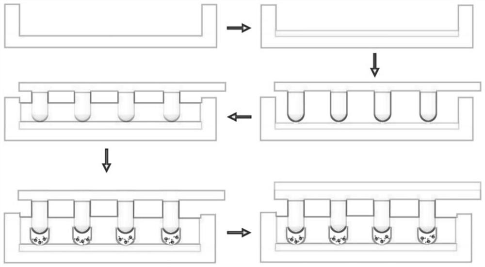
[0030] Such as figure 1 As shown, the present invention discloses a method for preparing a circulating cooling system based on nanometer confined hydraulic thermal effect, comprising the following steps:
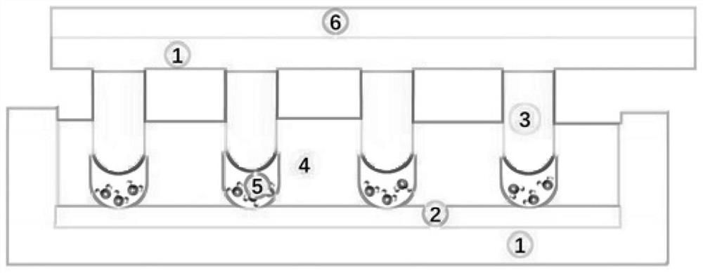
[0031] Step 1: integrating the electronic chip that needs to be dissipated on the silicon wafer, and the end surface of the silicon wafer away from the electronic chip is provided with an edge groove;
[0032] Step 2: depositing a confined layer with good thermal conductivity in the groove of the silicon wafer;
[0033] Step 3: Prepare a rigid nanocolumn array on the surface of the silicon wafer, and invert it on the groove of the silicon wafer, so that the nanocolumn array on the silicon wafer is located in the groove of the silicon wafer and in the groove restricted layer contact;
[0034] Step 4: Cast an epoxy resin film in the groove of the silicon wafer, separate the silicon wafer and the silicon wafer after cooling, so that the epoxy resin film on the restricted laye...
Embodiment 1
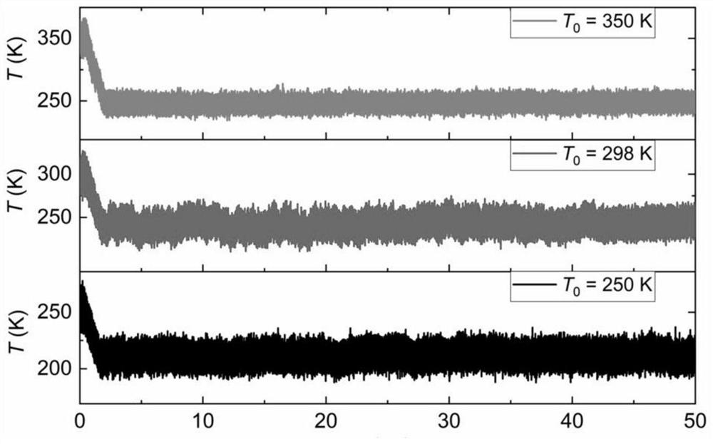
[0040] A graphene layer is used as a confined layer, capped carbon nanotubes are used as nanopillars, water is used as a cooling medium, and organic material vinylidene fluoride (PVDF) is used as a piezoelectric film. By applying an external electric field, the piezoelectric film will deform and drive the nanopillars to move up and down as a whole. in room temperature( T 0 = 298 K) When we reduce the distance between the nanopillars and the confinement layer, water molecules undergo a phase transition from disorder to order, and the temperature of water increases under adiabatic conditions, and the rising heat can pass through the nanopillars slowly Dissipate out; when we quickly separate the nanopillars and the confined layer, the water molecules will undergo an order-to-disorder phase transition, and the temperature of the water will drop, thereby realizing the cooling of the electronic chip integrated on the silicon wafer. Estimated by computer simulation, the adiabatic ...
Embodiment 2
[0042] A graphene layer is used as a confined layer, capped carbon nanotubes are used as nanopillars, water is used as a cooling medium, and organic material vinylidene fluoride (PVDF) is used as a piezoelectric film. By applying an external electric field, the piezoelectric film will deform and drive the nanopillars to move up and down as a whole. When the system is operating at a lower temperature, such as T 0=250 K, when we reduce the distance between the nanopillars and the confined layer, water molecules undergo a phase transition from disorder to order, which will generate a temperature rise, and the increased heat can be slowly released through the nanopillars Going out, when we rapidly increase the distance between the nanopillars and the confined layer, the water molecules will undergo an order-to-disorder phase transition, and the temperature of the water will drop, thereby realizing the cooling of the electronic chips integrated on the silicon wafer. Estimated by ...
PUM
 Abstract
Description
Claims
Application Information


