Preparation method of tantalum-doped large-area two-dimensional niobium disulfide material
A niobium disulfide, large-area technology, applied in metal material coating process, gaseous chemical plating, coating, etc., can solve the problems of difficult to accurately control the thickness and size, unable to prepare in batches, laborious, etc., and achieve good repeatability , convenient material acquisition method, high deposition rate effect
- Summary
- Abstract
- Description
- Claims
- Application Information
AI Technical Summary
Problems solved by technology
Method used
Image
Examples
Embodiment 1
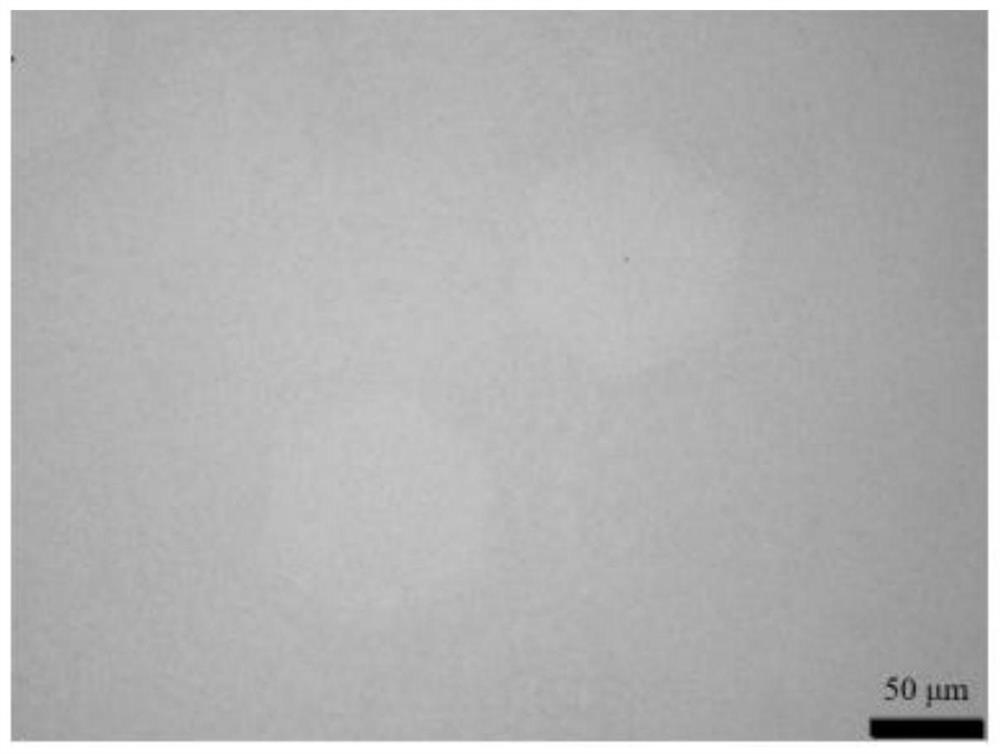
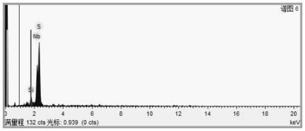
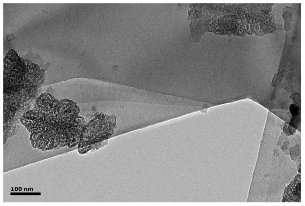
[0033] see Figure 1-5 As shown, a large-area two-dimensional niobium disulfide material, the large-area two-dimensional niobium disulfide material is made by the following steps:
[0034] Step S1: Paste 3M adhesive tape on the front and back surfaces of fluorphlogopite mica in the ultra-clean workbench, use a method similar to mechanical peeling, tear off the surface layer of the front and back surfaces of fluorophlogopite mica, and store it in an electronic drying box for future use ;Use acetone, isopropanol, and ethanol in sequence to ultrasonically clean the silicon wafer, and then cut it into 35×13mm with a silicon knife 2 Put it in the silicon wafer box for later use;
[0035] Step S2: Weigh 18mg of niobium pentoxide powder, 180mg of ammonium chloride powder and 200mg of sulfur powder respectively, put niobium pentoxide and ammonium chloride into a mortar and grind until the two are evenly mixed, then put the mixture In the quartz boat A, then place the sulfur powder i...
Embodiment 2
[0041] see Figure 6-10 Shown: a tantalum-doped large-area two-dimensional niobium disulfide material, the tantalum-doped large-area two-dimensional niobium disulfide material is made by the following steps:
[0042] Step S1: Paste 3M adhesive tape on the front and back surfaces of fluorphlogopite mica in the ultra-clean workbench, use a method similar to mechanical peeling, tear off the surface layer of the front and back surfaces of fluorophlogopite mica, and store it in an electronic drying box for future use ;Use acetone, isopropanol, and ethanol in sequence to ultrasonically clean the silicon wafer, and then cut it into 35×13mm with a silicon knife 2 Put it in the silicon wafer box for later use;
[0043]Step S2: Weigh 9mg of niobium pentoxide powder, 9mg of tantalum pentoxide powder, 180mg of ammonium chloride powder and 200mg of sulfur powder respectively, put niobium pentoxide, tantalum pentoxide and ammonium chloride into Grind in a mortar until the three are evenly...
PUM
 Abstract
Description
Claims
Application Information


