Design for improving stability of perovskite solar cell module

A technology of solar cells and battery modules, applied in the field of solar cells, can solve the problems of reduced module stability, increased parallel resistance, increased leakage current, etc., to achieve improved stability, high open circuit voltage and fill factor, and reduced leakage current Effect

Pending Publication Date: 2021-07-27
仁烁光能(苏州)有限公司
View PDF0 Cites 2 Cited by
  • Summary
  • Abstract
  • Description
  • Claims
  • Application Information

AI Technical Summary

Problems solved by technology

[0004] In the prior art, in the design process of the perovskite module, the design of P2 is often to cut the prepared extraction layer and the perovskite layer, so that part of the underlying transparent conductive electrode is exposed. However, this step is also The perovskite of the cut section will be exposed to the air. After the electrode is prepared, the electrode will be in direct contact with the perovskite layer at the section. Since the halogen in the perovskite is easy to diffuse and react with the electrode, it is easy to cause the module to fail. The stability is reduced, and the direct contact of the perovskite of the single-junction cell with the electrode will easily lead to an increase in parallel resistance and leakage, and the direct contact with the electrode of the multi-junction stack will easily lead to an increase in the leakage current due to the existence of the tunneling junction.

Method used


Image

  • Design for improving stability of perovskite solar cell module
  • Design for improving stability of perovskite solar cell module
  • Design for improving stability of perovskite solar cell module

Examples


Embodiment approach

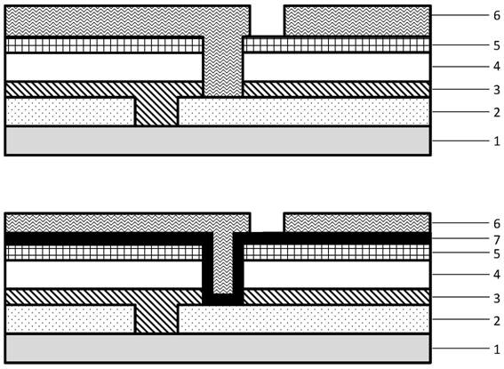
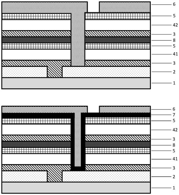
[0030]As an embodiment of the present invention, the battery module is divided into single-junction, double-junction stack and triple-junction stack; the single-junction battery module sequentially includes a conductive transparent substrate, A hole extraction layer 3, a perovskite layer 4, an electron extraction layer 5, a dense layer 7 and an electrode 6; the conductive transparent substrate sequentially includes a glass 1 and a transparent conductive film 2 from the light-receiving front to the light-receiving back; the double junction The battery module sequentially includes a transparent conductive substrate, a hole extraction layer 3, a wide-bandgap perovskite 41, an electron extraction layer 5, a tunneling composite layer 8, a hole extraction layer 3, and a narrow-bandgap calcium layer from the light-receiving front to the light-receiving back. The titanium ore 42, the electron extraction layer 5, the dense layer 7 and the electrode 6; the three-junction battery module s...

Embodiment 1

[0044] This Example 1 adopts figure 2 A large-area perovskite single-junction solar cell module is fabricated with the structure shown, and the specific fabrication process is as follows:

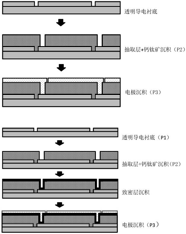
[0045] 1. Use laser to etch about 100um line width on the cleaned ITO substrate, which is P1.

[0046] 2. A layer of poly[bis(4-phenyl)(2,4,6-trimethylphenyl)amine] (PTAA) with a thickness of about 20 nm is used as the hole extraction layer.

[0047] 3. Deposit a layer of perovskite on the hole extraction layer with a thickness of about 300 nm.

[0048] 4. A layer of fullerene (C 60 ) as an electron extraction layer with a thickness of about 25 nm.

[0049] 5. A layer of 2,9-dimethyl-4,7-biphenyl-1,10-phenanthroline (BCP) was deposited by thermal evaporation with a thickness of about 7 nm.

[0050] 6. The line width of about 100um is used for laser etching, which is P2.

[0051] 7. Finally, a layer of Cu with a thickness of 150 nm was deposited by thermal evaporation as the conductive...

Embodiment 2

[0055] This embodiment 2 adopts figure 2 A large-area perovskite / perovskite tandem solar cell module group was prepared with the shown structure. The specific preparation process is as follows:

[0056] 1. Use laser to etch about 100um line width on the cleaned ITO substrate, which is P1.

[0057] 2. A layer of poly[bis(4-phenyl)(2,4,6-trimethylphenyl)amine] (PTAA) with a thickness of about 20 nm is used as the hole extraction layer.

[0058] 3. Deposit a layer of perovskite on the hole extraction layer with a thickness of about 300 nm.

[0059] 4. A layer of fullerene (C 60 ) as an electron extraction layer with a thickness of about 25 nm.

[0060] 5. Atomic layer deposition grows a layer of SnO 2 As a dense layer that hinders the diffusion of perovskite, the thickness is about 20 nm.

[0061] 6. The line width of about 100um is used for laser etching, which is P2.

[0062] 7. Finally, a layer of Cu with a thickness of 150 nm was deposited by thermal evaporation as the...


PUM

PropertyMeasurementUnit
thicknessaaaaaaaaaa
thicknessaaaaaaaaaa
thicknessaaaaaaaaaa

Abstract

The invention belongs to the technical field of solar cells, and particularly relates to a design for improving the stability of a perovskite solar cell module. The battery module is divided into a single-junction battery module, a double-junction battery module and a three-junction battery module, and compact layers are arranged in all the battery modules; each compact layer is located on a patterned perovskite layer, an electron extraction layer and a hole extraction layer, has good continuity and compactness, can perform shape-preserving growth on the patterned substrate to realize complete coverage, and has good electron transmission characteristics and conductivity, so that the normal ohmic contact between an electrode and a conductive film during series connection of the modules can be guaranteed. According to the present invention, the contact between the perovskite layer and the air and the metal electrode can be effectively blocked through the introduction of the compact layers, and when the compact layersare applied to the double-junction and three-junction perovskite laminated solar cell module groups, the introduction of the compact layers can effectively reduce a leakage current caused by the direct contact of a tunneling composite layer and the electrode, and finally the stable perovskite solar cell modules can be obtained.

Description

technical field [0001] The invention belongs to the technical field of solar cells, in particular to a design for improving the stability of a perovskite solar cell module. Background technique [0002] Perovskite solar cells are the fastest-growing type of third-generation new thin-film solar cells. They have increased from 3.8% to more than 25% in just a decade or so, and the cost of power generation of perovskite materials Compared with industrialized silicon solar cells, it is lower and the manufacturing process is simpler. It is considered to be the most commercial type of solar cell at present. [0003] However, to achieve high-efficiency large-area perovskite solar cells, it is necessary to overcome the large series resistance brought by the increase of the electrode area, which will lead to a decrease in the device fill factor and ultimately lead to a decrease in the efficiency of large-area devices. Therefore, when preparing larger-area devices, the whole large-are...

Claims


Application Information

Patent Timeline
Patent Type & Authority Applications(China)
IPC IPC(8): H01L51/42H01L51/44H01L51/48H01L27/30
CPCH10K30/57H10K30/15H10K30/81H10K30/88Y02E10/549
Inventor 谭海仁肖科
Owner 仁烁光能(苏州)有限公司
Why Eureka
Try Eureka