Regeneration processing method of substrate slice after SOI bonding process

A processing method and a bonding technology, which are applied in the field of recycling and processing of integrated circuit single crystal silicon polished wafers, can solve problems such as roughness, surface damage, and ineffective recycling of substrate wafers, and achieve the effects of reducing costs and increasing yield

Active Publication Date: 2021-07-30
MCL ELECTRONICS MATERIALS
View PDF10 Cites 0 Cited by
  • Summary
  • Abstract
  • Description
  • Claims
  • Application Information

AI Technical Summary

Problems solved by technology

Since the front of the substrate is quite rough compared to the original silicon substrate, there will be some damage on the surface, and there is an oxide film growing on the entire back and front edge 2mm before bonding, which cannot be directly used for re-bondi

Method used


Image

  • Regeneration processing method of substrate slice after SOI bonding process
  • Regeneration processing method of substrate slice after SOI bonding process

Examples


Embodiment 1

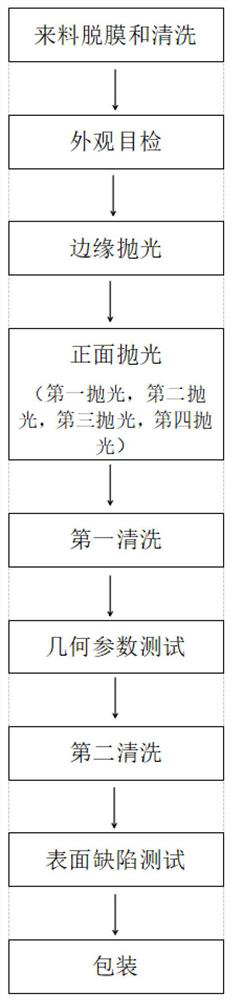
[0034] 1) Put the substrate sheet into the tetrafluoro film box, use HF solution to soak and remove the film for 5 minutes in the etching machine, the volume ratio of hydrofluoric acid and pure water in the HF solution is 1:20; then use ammonia water, The mixture of hydrogen peroxide and pure water was washed for 5 minutes at a temperature of 50° C., and the volume ratio of ammonia water, hydrogen peroxide and pure water was 1:2:20.

[0035] 2) Carry out manual appearance visual inspection under a strong light with a light intensity of 160,000 LX to confirm that the oxide film has been completely peeled off, and pick out edge chips that may cause fragments in subsequent processing.

[0036] 3) The edge of the substrate is polished, and the substrate is fixed on the vacuum chuck during the edge polishing process, and the polishing cloth with a hardness of 60 is used to polish the substrate, the polishing inclination angle is 50 degrees, the edge polishing pressure is 80N, and th...

Embodiment 2

[0050] 1) Put the substrate sheet into the tetrafluoro film box, and use HF solution to soak and remove the film for 10 minutes in the etching machine. The volume ratio of hydrofluoric acid and pure water in the HF solution is 1:30; then use ammonia water, The mixture of hydrogen peroxide and pure water was washed for 10 minutes at a temperature of 80° C., and the volume ratio of ammonia water, hydrogen peroxide and pure water was 1:1:30.

[0051] 2) Carry out manual appearance visual inspection under a strong light with a light intensity of 160,000 LX to confirm that the oxide film has been completely peeled off, and pick out edge chips that may cause fragments in subsequent processing.

[0052] 3) The edge of the substrate is polished, the substrate is fixed on the vacuum chuck during the edge polishing process, and the polishing cloth with a hardness of 80 is used to polish the substrate, the polishing inclination angle is 50 degrees, the edge polishing pressure is 120N, and...


PUM


Abstract

The invention belongs to the technical field of recycling and processing of monocrystalline silicon polished wafers of integrated circuits, and particularly relates to a regeneration processing method of a substrate slice after an SOI bonding process. The method comprises the following steps: demoulding and cleaning a recovered SOI substrate slice, polishing the front surface of the substrate slice, cleaning the substrate slice for the first time, testing the flatness uniformity and thickness of the substrate slice, and cleaning the substrate slice for the second time. According to the regeneration processing method disclosed by the invention, the recovery of the substrate slice after the SOI bonding process is realized, so that the substrate slice reaches a substrate silicon slice with a high surface quality level again, the substrate slice can be circularly used for multiple times in the SOI bonding process, and the processing cost is far lower than the price of purchasing a new substrate silicon slice.

Description

technical field [0001] The invention belongs to the technical field of recovery and processing of integrated circuit monocrystalline silicon polished wafers, and in particular relates to a regeneration processing method of substrate wafers after an SOI bonding process. Background technique [0002] Single crystal silicon polished wafer is a widely used semiconductor material, which can be used as a substrate for manufacturing SOI (Silicon-On-Insulator, silicon on insulating substrate) materials, SOI is a functional integrated circuit substrate It is a material in which a single crystal silicon film is grown on an insulating substrate, or a single crystal silicon film is separated from a silicon substrate by an insulating layer. It is an ideal material for manufacturing MOS transistors. With the development of ultra-large-scale integrated circuits, in order to reduce the cost of chip manufacturing, domestically mainly use polished single crystal silicon wafers with a diameter...

Claims


Application Information

Patent Timeline
IPC IPC(8): H01L21/02H01L21/683
CPCH01L21/02032H01L21/02013H01L21/6835H01L2221/68345H01L2221/68377
Inventor 熊诚雷赵文龙李战国胡晓亮邵奇
Owner MCL ELECTRONICS MATERIALS
Why Eureka
Try Eureka