Low-loss integrated bent optical waveguide and design method thereof
A design method and optical waveguide technology, applied in the field of integrated optics, can solve problems such as scattering loss, increased bending loss, and complicated manufacturing process, and achieve the effect of improving design flexibility and reducing bending loss
- Summary
- Abstract
- Description
- Claims
- Application Information
AI Technical Summary
Problems solved by technology
Method used
Image

Examples
Embodiment Construction
[0036] In order to make the purpose and technical solution of the patent of the present invention clearer, it will be described in detail in combination with the following embodiments and with reference to the accompanying drawings.
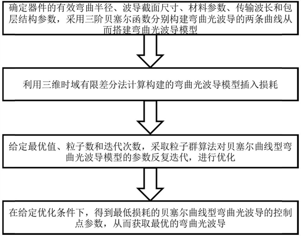
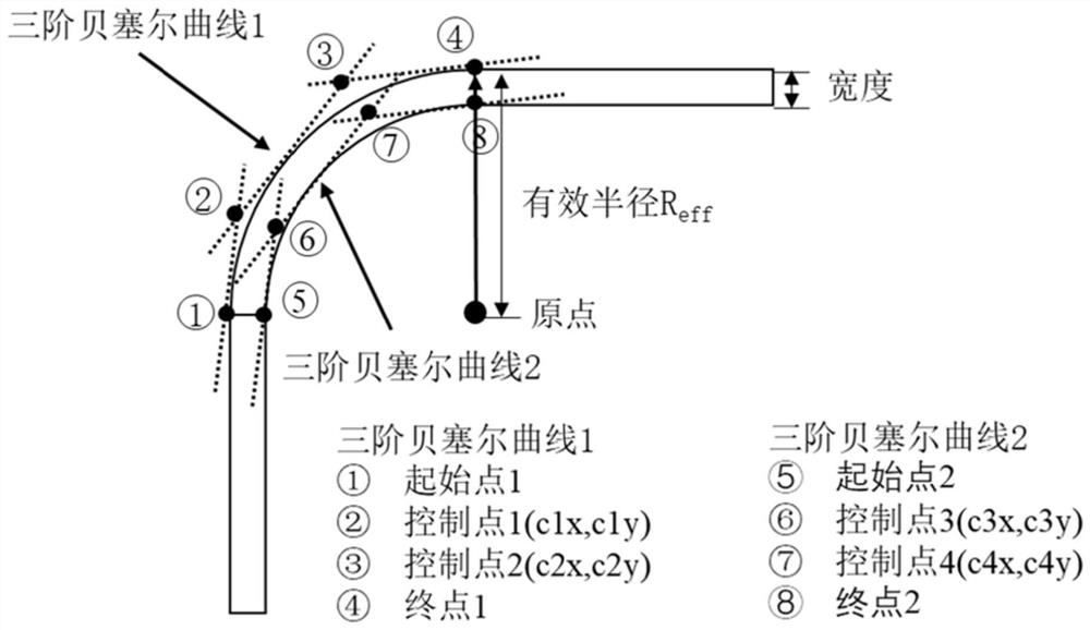
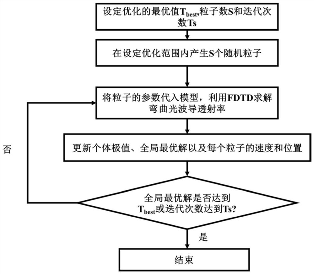
[0037] Such as figure 1 As shown, the present invention provides a low-loss integrated curved optical waveguide design method, that is, a method for optimizing the shape of the curved optical waveguide, which is used to optimize the boundary curve of the curved optical waveguide to reduce the waveguide loss as much as possible. A curved optical waveguide refers to an optical waveguide that is curved on a plane. A common curved optical waveguide is an arc-shaped optical waveguide, but in the present invention, its insertion loss can be further reduced by optimizing its shape.
[0038] The steps of the low-loss integrated curved optical waveguide design method are as follows:
[0039] S1. Obtain the effective bending radius, waveguide cross-sectio...
PUM
 Abstract
Description
Claims
Application Information
 - R&D
- Intellectual Property
- Life Sciences
- Materials
- Tech Scout
- Unparalleled Data Quality
- Higher Quality Content
- 60% Fewer Hallucinations
Browse by: Latest US Patents, China's latest patents, Technical Efficacy Thesaurus, Application Domain, Technology Topic, Popular Technical Reports.
© 2025 PatSnap. All rights reserved.Legal|Privacy policy|Modern Slavery Act Transparency Statement|Sitemap|About US| Contact US: help@patsnap.com