Silicon-based graphene photodetector array and its cmos three-dimensional integration method

A photoelectric detection and graphene technology, applied in circuits, electrical components, electrical solid devices, etc., can solve the problems of difficult to continue to improve performance, and achieve the effects of simple timing, low cost, and excellent thermal conductivity.

Active Publication Date: 2022-06-24
ZHEJIANG UNIV
View PDF0 Cites 0 Cited by
  • Summary
  • Abstract
  • Description
  • Claims
  • Application Information

AI Technical Summary

Problems solved by technology

The traditional silicon-based CMOS process is gradually approaching its performance limit at the sub-10nm technology node. Due to the limitations of physical laws and manufacturing costs, it is difficult to continue to improve performance

Method used


Image

  • Silicon-based graphene photodetector array and its cmos three-dimensional integration method
  • Silicon-based graphene photodetector array and its cmos three-dimensional integration method
  • Silicon-based graphene photodetector array and its cmos three-dimensional integration method

Examples


Embodiment Construction

[0029] The technical solutions in the embodiments of the present invention will be completely described below with reference to the accompanying drawings in the embodiments of the present invention. Obviously, the described embodiments are only a part of the embodiments of the present invention, rather than all the embodiments. Based on the embodiments of the present invention, all other embodiments obtained by those of ordinary skill in the art without creative efforts shall fall within the protection scope of the present invention.

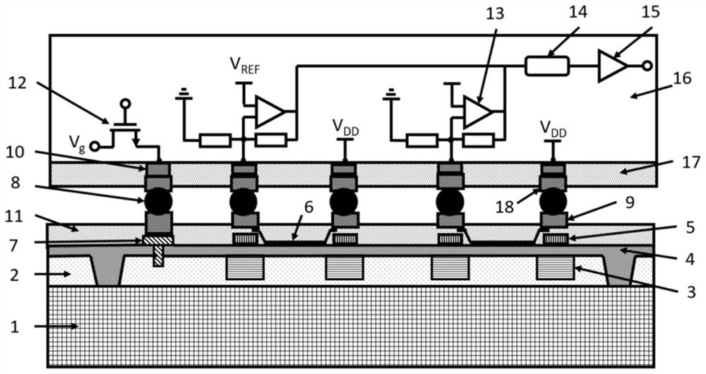
[0030] like figure 1 As shown, a silicon-based graphene photodetection array provided by the present invention sequentially includes a p-type semiconductor silicon substrate 1, an N-well 2, an oxide insulating layer 4, a first passivation layer 11, a second passivation layer from bottom to top The N-well 2 is deposited to form the isolation layer 3; the oxide insulating layer 4 is provided with a gate through hole 7, and the upper surface is pro...


PUM

PropertyMeasurementUnit
thicknessaaaaaaaaaa
thicknessaaaaaaaaaa
electron mobilityaaaaaaaaaa

Abstract

The invention discloses a silicon-based graphene photodetection array and a CMOS three-dimensional integration method thereof. The silicon-based graphene photodetection array adopts a p-type silicon substrate, including a gate, a semiconductor silicon substrate, an oxide insulating layer and Single-layer graphene film, etc.; the photosensitive pixel area unit and the external area in the array device are isolated by LOCOS technology to achieve low crosstalk effect of small-sized array; Effective integration of the readout circuit chip and excellent heat conduction; CMOS readout circuit adopts transimpedance amplifier, sampling amplifier and analog-to-digital converter for high-quality, low-noise signal output. The invention realizes the combination of graphene and traditional CMOS integration technology, broadens the spectral response range, improves imaging quality and expands application scenarios in the field of photoelectric detection.

Description

technical field [0001] The invention belongs to the technical field of image sensors, relates to an image sensor device structure, and in particular relates to a silicon-based graphene photodetection array and a CMOS (complementary metal oxide semiconductor) three-dimensional integration method. Background technique [0002] The photodetector can sense light and convert the analog signal current. After signal processing, image acquisition, transmission and processing can be realized. Photodetectors have good photosensitive efficiency and extremely high imaging quality, and are widely used in high-end imaging chemical material analysis, medical and health, space technology and other fields. At present, the mainstream photodetector manufacturing technology is mainly based on the traditional silicon-based CMOS process, which has the advantages of low cost, high integration density, and good compatibility. The traditional silicon-based CMOS process is gradually approaching its ...

Claims


Application Information

Patent Timeline
Patent Type & Authority Patents(China)
IPC IPC(8): H01L27/146
CPCH01L27/14689H01L27/1469H01L27/1461H01L27/14609H01L27/14636H01L27/1463
Inventor 徐杨刘亦伦吕建杭董云帆刘粒祥俞滨
Owner ZHEJIANG UNIV
Why Eureka
Try Eureka