Light-emitting diode based on CsPbI3 material
A technology of light-emitting diodes and substrates, applied in the manufacture of electrical components, electrical solid devices, semiconductor/solid devices, etc., can solve the problems of difficult large-area and flexible device preparation, short life, low efficiency, etc., to achieve light color stability, The preparation process is simple and the effect of improving luminous efficiency
- Summary
- Abstract
- Description
- Claims
- Application Information
AI Technical Summary
Problems solved by technology
Method used
Image
Examples
Embodiment 1
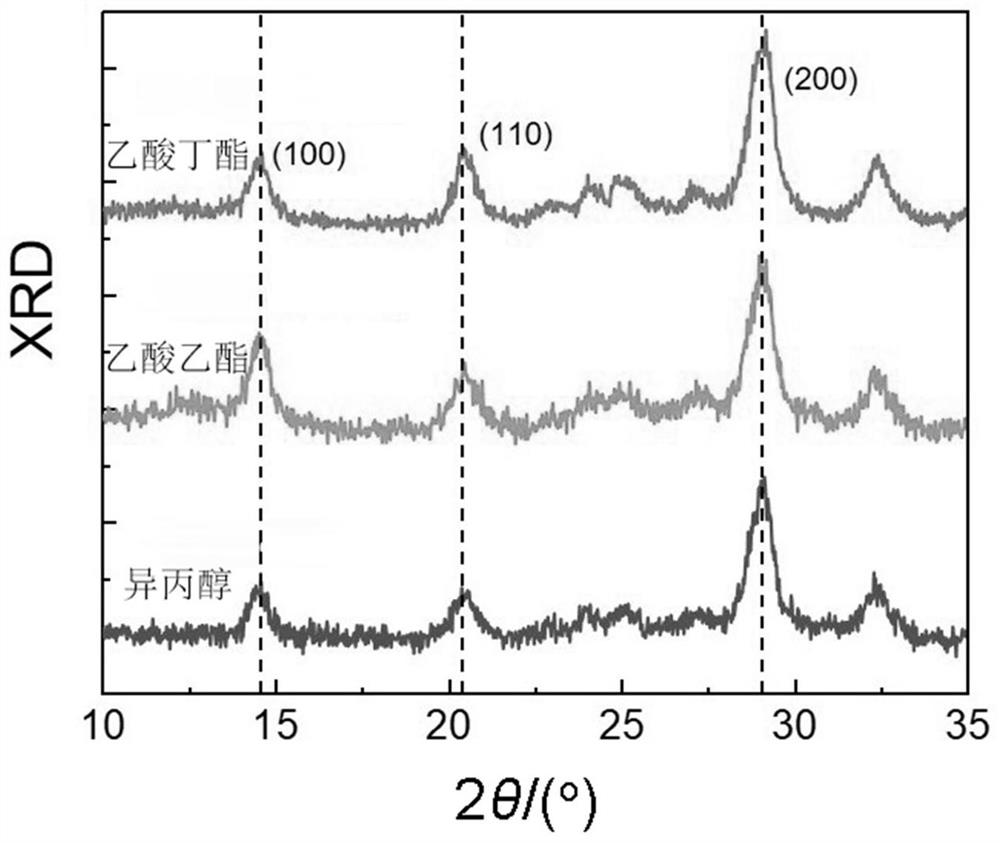
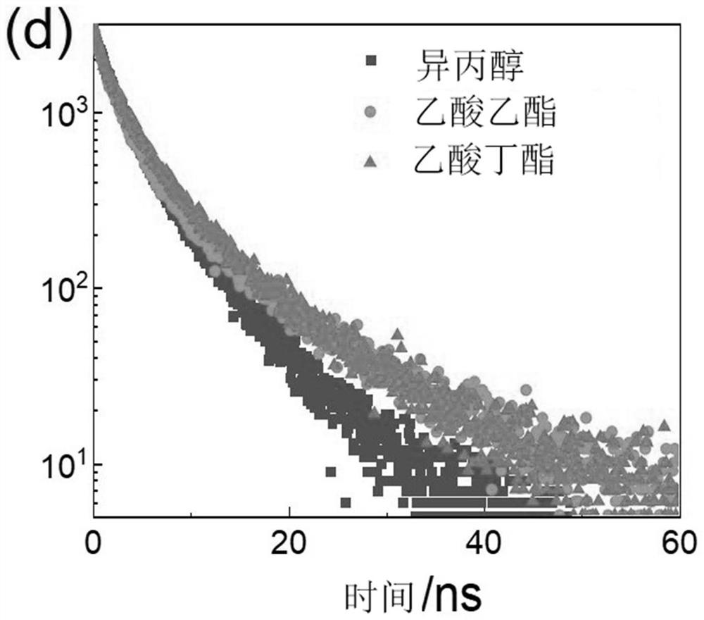
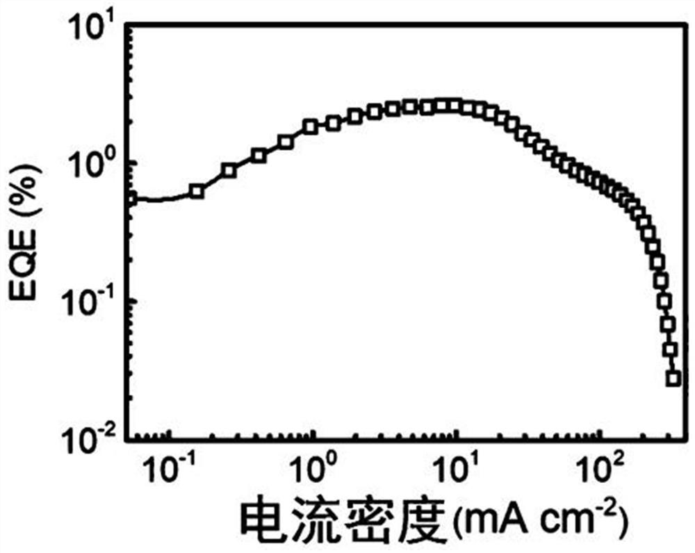
[0029] see Figure 1-4 As shown, the present embodiment relates to a light-emitting diode based on CsPbI3 material, and the specific implementation steps are as follows:
[0030] Step 1: Carry out standardized cleaning of the transparent conductive glass substrate (first rinse with deionized water, then repeatedly ultrasonically clean three times with deionized water, acetone, and ethanol, and then dry for 20 minutes. Ultraviolet ozone pretreatment Time is 20min) after drying, prepare transparent conductive glass as the anode substrate;
[0031] Step 2, prepare the perovskite precursor solution, dissolve PEABr, NPABr2, CsBr and PbBr2 in the organic solution; use the spin coating method, the spin coating speed is 2000-6000rpm for coating, and the conductive glass is heated and kept at the required heat of 120 ℃, heat the perovskite precursor solution and spin-coat the substrate surface, then drop chlorobenzo and spin-coat to obtain the first perovskite layer, and anneal for 2 ...
Embodiment 2
[0034] Using the same process as in Example 1, the difference is that in step 2, CH3NH3PbI3 with a mass ratio of 2.5% and CH3NH3PbBr3 with a mass ratio of 1.25% can be used to mix two different systems of perovskite precursor solutions according to a molar ratio of 0.3:2.7 to obtain a Perovskite solution with yellow light.
Embodiment 3
[0036] The preparation method is the same as that in Example 1, the difference is that in step 3, in the perovskite precursor solution, the ratio of each component is adjusted to m=0.8, c=0, n=1.
PUM
| Property | Measurement | Unit |
|---|---|---|
| thickness | aaaaa | aaaaa |
| thickness | aaaaa | aaaaa |
Abstract
Description
Claims
Application Information


