Preparation method of high-brightness infrared light emitting diode core and diode core

A technology of light-emitting diodes and infrared light, which is applied to electrical components, circuits, semiconductor devices, etc., and can solve the problems of cumbersome finger pattern production, high cost, and numerous steps

Pending Publication Date: 2021-08-31
SHANDONG INSPUR HUAGUANG OPTOELECTRONICS
View PDF17 Cites 0 Cited by
  • Summary
  • Abstract
  • Description
  • Claims
  • Application Information

AI Technical Summary

Problems solved by technology

Although the ITO finger electrode can effectively reduce the absorption of light, its adhesion to semiconductor materials is much worse than that of the point electrode, and no m...

Method used


Image

  • Preparation method of high-brightness infrared light emitting diode core and diode core
  • Preparation method of high-brightness infrared light emitting diode core and diode core
  • Preparation method of high-brightness infrared light emitting diode core and diode core

Examples


Embodiment 1

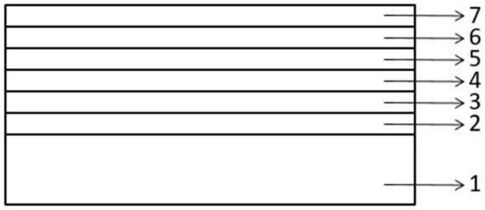
[0041] A method for preparing a high-brightness infrared light-emitting diode tube core, such as Figure 1-3 As shown, the specific steps are as follows:

[0042] (1) Wafer thinning: use photoresist to protect the front of the wafer with the epitaxial layer, and chemically polish the back with an etching solution. GaAs substrate, N-type GaAs, N-type confinement layer, MQW quantum well layer, P-type confinement layer, P-type GaAs, P-type GaP contact layer, where the back of the wafer is a GaAs substrate, and the front of the wafer is a P-type GaP contact layer ; The epitaxial layer includes N-type GaAs, N-type confinement layer, MQW quantum well layer, P-type confinement layer, P-type GaAs, and P-type GaP contact layer from bottom to top.

[0043] The corrosion solution is a mixed solution of sulfuric acid, hydrogen peroxide and water, the ratio of the corrosion solution is sulfuric acid: hydrogen peroxide: water = 5:1:1, wherein the density of sulfuric acid is 1.84g / ml, the c...

Embodiment 2

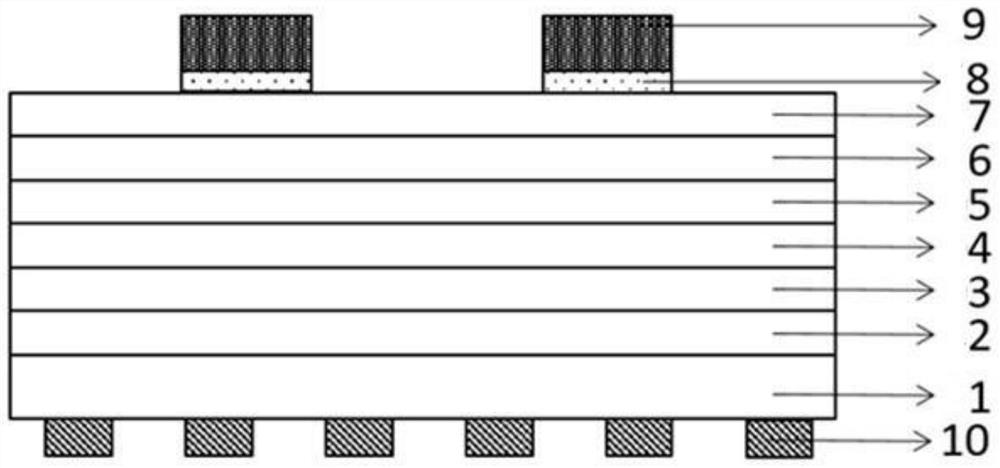
[0053] A high-brightness infrared light-emitting diode tube core is made by the preparation method of Example 1, and its structure is as follows: Figure 4 As shown, from bottom to top are adhesive film, N-side electrode, GaAs substrate, epitaxial layer, ohmic contact layer, and P-side electrode; the epitaxial layer includes N-type GaAs, N-type confinement layer, and MQW quantum well layer from bottom to top , P-type confinement layer, P-type GaAs, P-type GaP contact layer.

Embodiment 3

[0055] A method for preparing a high-brightness infrared light-emitting diode die. The difference from Embodiment 1 is that AuBe is manufactured in step (2), and the thickness is 1000 angstroms.


PUM

PropertyMeasurementUnit
Densityaaaaaaaaaa
Densityaaaaaaaaaa
Thicknessaaaaaaaaaa

Abstract

The invention relates to a preparation method of a high-brightness infrared light emitting diode core and a diode core. The preparation method comprises the following steps of thinning a wafer, manufacturing an ohmic contact layer and an electrode layer, manufacturing an electrode pattern, cutting the diode core and coarsening to obtain an adhesive film, an N-surface electrode, a GaAs substrate, an epitaxial layer, an ohmic contact layer and a P-surface electrode from bottom to top in sequence. The epitaxial layer comprises the diode core of the N-type GaAs, the N-type limiting layer, the MQW quantum well layer, the P-type limiting layer, the P-type GaAs and the P-type GaP contact layer from bottom to top, the cost is greatly reduced, and the brightness is obviously improved.

Description

technical field [0001] The invention relates to a method for preparing a high-brightness infrared light-emitting diode tube core and the diode tube core, belonging to the technical field of semiconductor light-emitting diode manufacturing. Background technique [0002] Gallium arsenide is an important semiconductor material with a lattice constant of 5.65×10⁻¹⁰m, a melting point of 1237°C, and a band gap of 1.4 electron volts. It is a typical energy band structure material capable of direct transition, and its conduction band minimum Both the maximum value of the valence band and the valence band are in the center of the Brillouin zone, which makes it have a high electro-optical conversion efficiency and is an excellent material for the preparation of optoelectronic devices. Compared with traditional silicon semiconductor materials, gallium arsenide materials have many advantages such as high electron mobility, large band gap, direct band gap, and low power consumption. The ...

Claims


Application Information

Patent Timeline
IPC IPC(8): H01L33/00H01L33/06H01L33/14
CPCH01L33/145H01L33/06H01L33/0062
Inventor 徐晓强程昌辉王梦雪闫宝华
Owner SHANDONG INSPUR HUAGUANG OPTOELECTRONICS
Why Eureka
Try Eureka