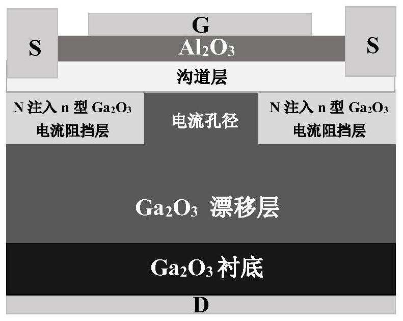
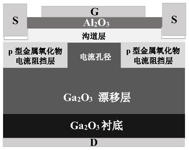
P-type metal oxide current blocking layer Ga2O3 vertical metal oxide semiconductor field effect transistor
A field-effect transistor, oxide semiconductor technology, applied in semiconductor devices, semiconductor/solid-state device manufacturing, circuits, etc., can solve problems such as limiting device application, low breakdown voltage, and inability to form pn junctions in devices to improve breakdown. voltage, the effect of increasing the breakdown voltage
- Summary
- Abstract
- Description
- Claims
- Application Information
AI Technical Summary
Problems solved by technology
Method used
Image

Examples
Embodiment 1
[0038] Example 1: The preparation thickness is 2um, and the doping concentration is 2×10 18 cm -3 The p-type tin oxide current blocking layer gallium oxide vertical MOSFET.
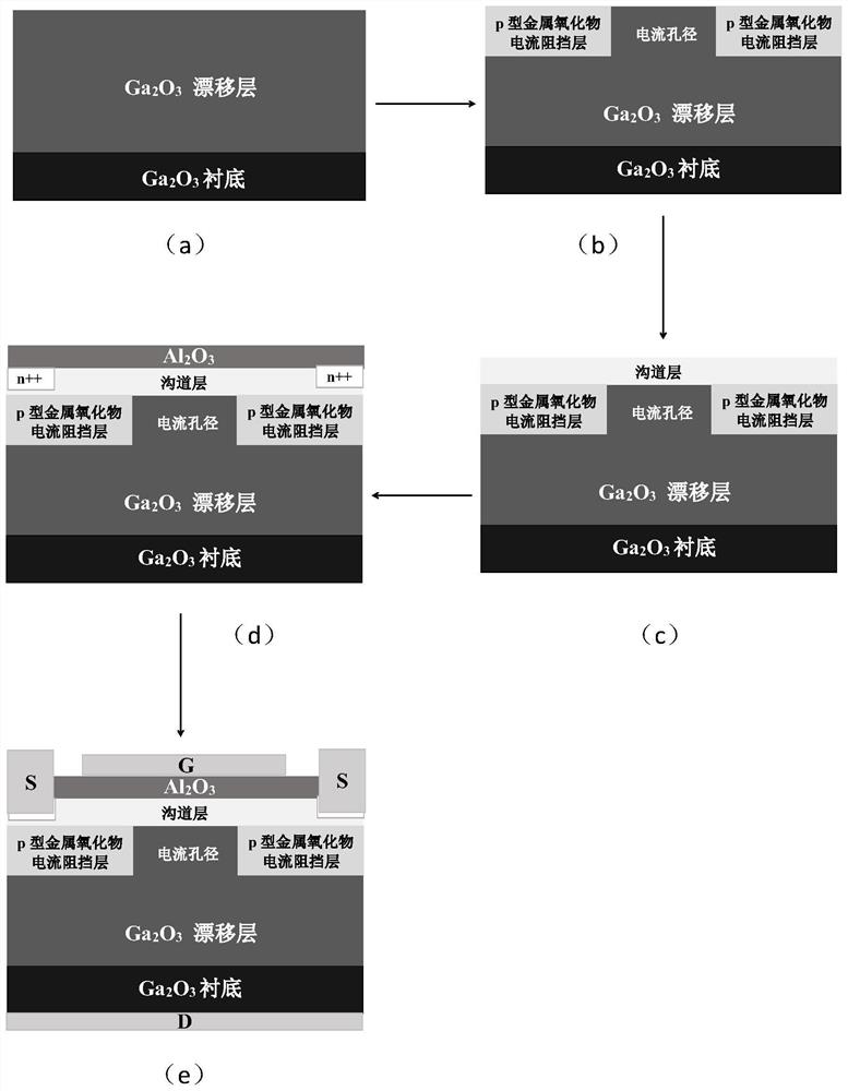
[0039] Step 1, growing a gallium oxide drift layer on a gallium oxide substrate, such as image 3 (a).
[0040] Select a Sn-doped gallium oxide (001) substrate and clean it; 2 Under the atmosphere, GaCl and O are introduced into the reaction chamber 2 , a silicon-doped gallium oxide drift layer was deposited on the substrate by hydride vapor phase epitaxy, where the proportion of GaCl to the mixed gas was 0.2, and the flow rate was 60slm;
[0041] Silicon ions are implanted in the gallium oxide drift layer by ion implantation technology, and the implantation dose is 5×10 13 cm -3 , with an implant energy of 600keV, and at 800°C N 2 Annealing for 1min under atmosphere to activate impurities;
[0042] For grown Ga 2 o 3 The drift layer is chemically mechanically polished to remove surface pits gen...
Embodiment 2
[0053] Example 2: The preparation thickness is 1um, and the doping concentration is 7×10 17 cm -3 The p-type nickel oxide current blocking layer gallium oxide vertical MOSFET.
[0054] Step 1, growing a gallium oxide drift layer on a gallium oxide substrate, such as image 3 (a).
[0055] 1.1) Select a Sn-doped gallium oxide (001) substrate and clean it; 2 Under the atmosphere, GaCl and O are introduced into the reaction chamber 2 , Deposit a silicon-doped gallium oxide drift layer on the substrate by hydride vapor phase epitaxy, where the ratio of GaCl to the mixed gas is 0.4, and the flow rate is 60slm;
[0056] 1.2) By ion implantation technology, silicon ions are implanted in the gallium oxide drift layer, and the implant dose is 6×10 13 cm -3 , with an implant energy of 600keV, and at 800°C N 2 Annealing for 1min under atmosphere to activate impurities;
[0057] 1.3) For grown Ga 2 o 3 The drift layer is chemically mechanically polished to remove surface pits ge...
Embodiment 3
[0071] Example 3: The preparation thickness is 0.2um, and the doping concentration is 2×10 17 cm -3 The p-type cuprous oxide current blocking layer gallium oxide vertical MOSFET.
[0072] Step A, growing a gallium oxide drift layer on a gallium oxide substrate, such as image 3 (a).
[0073] Select a Sn-doped gallium oxide (001) substrate and clean it; 2 Under the atmosphere, GaCl and O are introduced into the reaction chamber 2 , Deposit a silicon-doped gallium oxide drift layer on the substrate by hydride vapor phase epitaxy, where the ratio of GaCl to the mixed gas is 0.1, and the flow rate is 30slm;
[0074] Then, through ion implantation technology, silicon ions are implanted in the gallium oxide drift layer, and the implantation dose is 8×10 13 cm -3 , with an implant energy of 600keV, and at 800°C N 2 Annealing for 1min under atmosphere to activate impurities;
[0075] For grown Ga 2 o 3 The drift layer is chemically mechanically polished to remove surface pit...
PUM
| Property | Measurement | Unit |
|---|---|---|
| Thickness | aaaaa | aaaaa |
| Thickness | aaaaa | aaaaa |
| Thickness | aaaaa | aaaaa |
Abstract
Description
Claims
Application Information
 - R&D
- Intellectual Property
- Life Sciences
- Materials
- Tech Scout
- Unparalleled Data Quality
- Higher Quality Content
- 60% Fewer Hallucinations
Browse by: Latest US Patents, China's latest patents, Technical Efficacy Thesaurus, Application Domain, Technology Topic, Popular Technical Reports.
© 2025 PatSnap. All rights reserved.Legal|Privacy policy|Modern Slavery Act Transparency Statement|Sitemap|About US| Contact US: help@patsnap.com