

Semiconductor epitaxial wafer and method for manufacturing same
A technology of epitaxial wafers and manufacturing methods, applied in semiconductor/solid-state device manufacturing, semiconductor devices, electrical components, etc., can solve problems such as insufficient, heavy metal pollution of semiconductor substrates, etc., and achieve the effect of high gettering capacity
- Summary
- Abstract
- Description
- Claims
- Application Information
AI Technical Summary
Problems solved by technology
Method used
Image

Examples
Embodiment
[0076] (invention example)
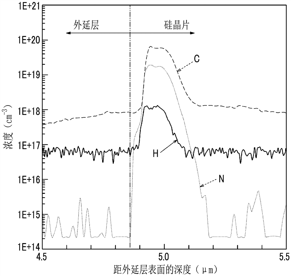
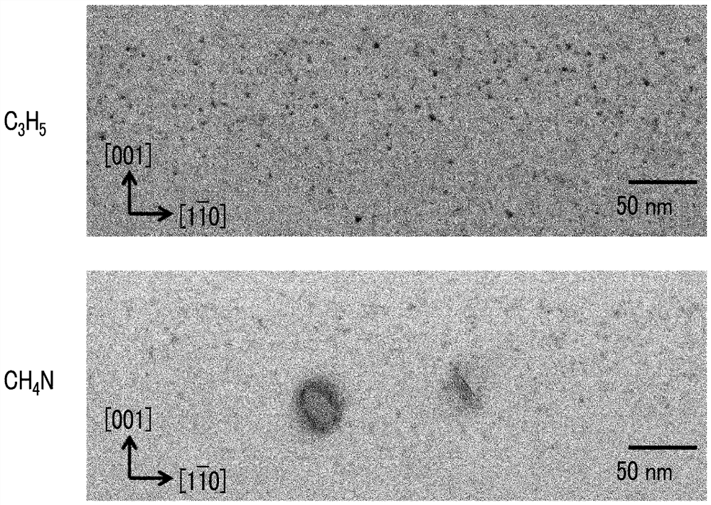
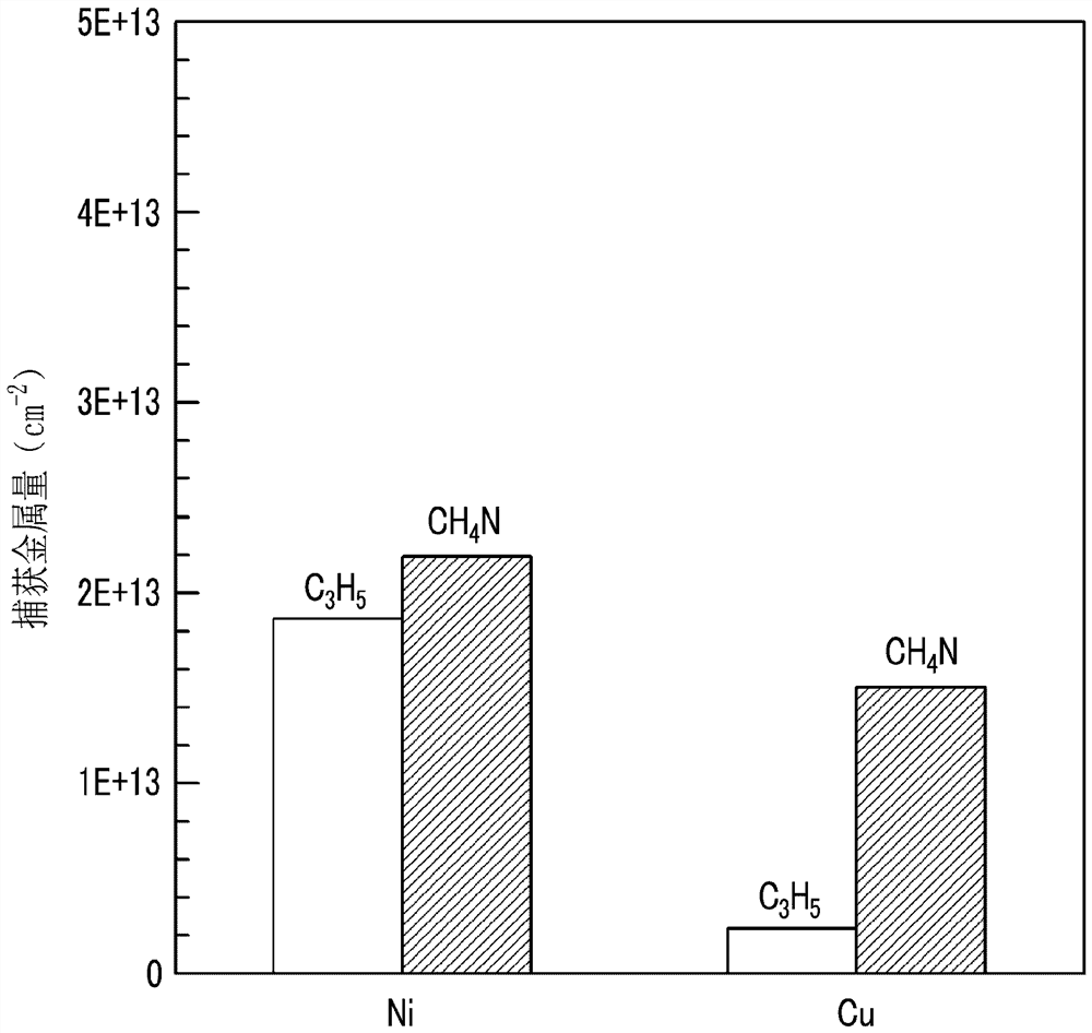
[0077] An n-type silicon wafer (diameter: 300 mm, thickness: 775 μm, dopant type: phosphorus, resistivity: 20 Ω·cm) obtained from a CZ single crystal silicon ingot was prepared. Next, using a cluster ion generator (manufactured by NISSIN ION EQUIPMENT CO.LTD., CLARIS (registered trademark)), using propylamine (C 3 h 9 N) As a raw material gas, generate and extract CH 4 N cluster ions at an accelerating voltage of 80keV / Cluster (the accelerating voltage per carbon atom is 32keV / atom, the accelerating voltage per hydrogen atom is 2.7keV / atom, and the accelerating voltage per nitrogen atom is 37.3keV / atom) The surface of the silicon wafer is irradiated under the irradiation condition. In addition, the dose when irradiating cluster ions was set to 1.0×10 15 ions / cm 2 . Converted to the number of carbon atoms is 1.0×10 15 atoms / cm 2 , converted to the number of hydrogen atoms is 4.0×10 15 atoms / cm 2 , converted to the number of nitrogen atoms ...
PUM
| Property | Measurement | Unit |
|---|---|---|
| Half width | aaaaa | aaaaa |
| Thickness | aaaaa | aaaaa |
| Resistivity | aaaaa | aaaaa |
Abstract
Description
Claims
Application Information