Transistor device with stretchable field effect, preparation method thereof and product

A transistor and field effect technology, applied in the field of transistor devices and their preparation, can solve the problems of easy cracking, limited application range of flexible devices, small strain range, etc., and achieve good switching performance, great application potential and promotion value, The Effect of Good Light Response

Pending Publication Date: 2021-10-01
INST OF PHYSICS - CHINESE ACAD OF SCI
View PDF10 Cites 0 Cited by
  • Summary
  • Abstract
  • Description
  • Claims
  • Application Information

AI Technical Summary

Problems solved by technology

[0004] However, compared with organic materials, two-dimensional semiconductor materials are more prone to fragmentation when the deformation is large. Most of the existing technical methods can only ensure that the device can work under bending conditions. The strain range applied by bending is very small, so that the flexible device limited range of applications

Method used


Image

  • Transistor device with stretchable field effect, preparation method thereof and product
  • Transistor device with stretchable field effect, preparation method thereof and product
  • Transistor device with stretchable field effect, preparation method thereof and product

Examples


Embodiment 1

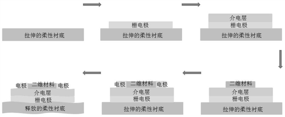
[0097] As an example, this embodiment is used to illustrate the preparation of the transistor device with stretchable field effect of the present invention.

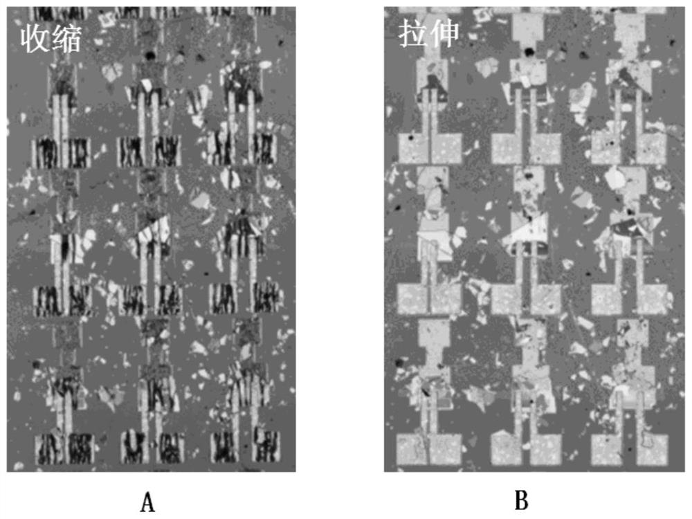
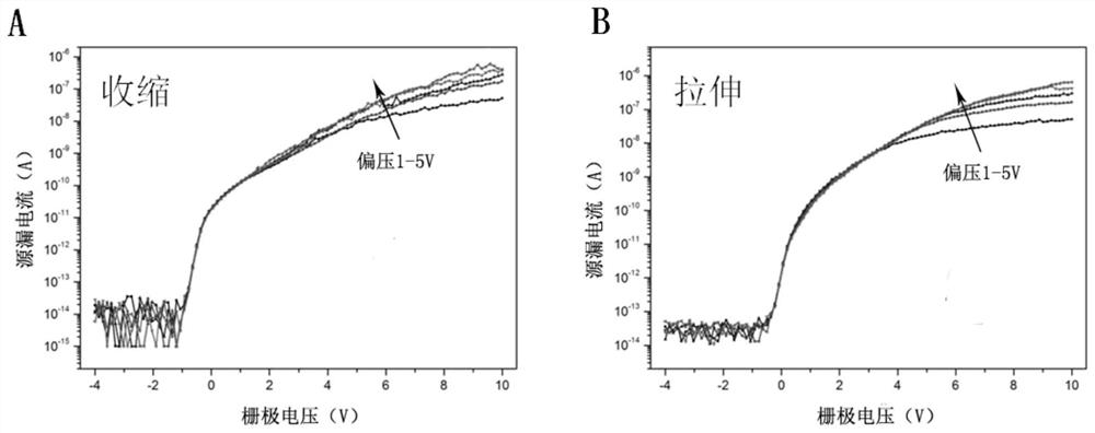
[0098] figure 1 It is a schematic diagram of the preparation process of the transistor device with stretchable field effect of the present invention. As shown in the figure, the preparation method of the present invention comprises the following steps in sequence:

[0099] (1) The flexible substrate is pre-stretched, and the flexible substrate used is PDMS. Stretch 5%.

[0100] (2) Paste a PET mask on the stretched substrate, and the mask is prepared by ultraviolet lithography and inductively coupled plasma etching. 2 nm titanium and 10 nm gold were deposited as gate electrodes by electron beam evaporation.

[0101] (3) Transfer boron nitride on the gate electrode with a thickness of 40 nanometers.

[0102] (4) Molybdenum disulfide thin film grown on sapphire substrate by chemical vapor deposition method, the surfac...


PUM

PropertyMeasurementUnit
thicknessaaaaaaaaaa
thicknessaaaaaaaaaa
thicknessaaaaaaaaaa

Abstract

The invention provides a transistor device with a stretchable field effect. The device comprises a stretchable flexible substrate, a deposited metal gate electrode, a two-dimensional insulating material and/or a flexible dielectric layer, a two-dimensional semiconductor material grown on the flexible substrate, and a source-drain metal electrode. The invention also provides a preparation method and application of the device. The manufacturing method of the device is improved, the flexible substrate of the device to be manufactured is pre-stretched and fixed, and then the two-dimensional semiconductor material is directly transferred on the stretched substrate to manufacture the device. The two-dimensional semiconductor material such as molybdenum disulfide is used as a channel material of the device, and the two-dimensional insulating material such as boron nitride is used as a dielectric layer of the device. After the device is manufactured, the substrate is released, the material on the substrate is shrunk, and the stretchable device of the wrinkle structure is formed. The stable field effect transistor three-terminal device is successfully prepared and can be applied to logic circuits, photoelectric detection and nerve synaptic morphological devices. The problem that a two-dimensional semiconductor material flexible device cannot bear large strain and cannot work stably under the strain condition is effectively solved.

Description

technical field [0001] The present invention generally relates to the fields of micro-nano processing and semiconductor manufacturing, and in particular to a transistor device with stretchable field effect and its preparation method and product. Background technique [0002] Flexible devices are the development trend of the next generation of new devices. Because of their softness and flexibility, they can be applied to various sensors, wearable devices, etc., opening up new research directions for electronic devices in biomedicine and artificial intelligence. [0003] Most of the current flexible devices use organic materials, the preparation process is highly toxic, and the device performance is not high. The emergence of two-dimensional semiconductor materials provides a new idea for the preparation of flexible devices. Using two-dimensional semiconductor materials can not only prepare simple two-terminal devices, but also three-terminal field-effect transistor devices an...

Claims


Application Information

Patent Timeline
Patent Type & Authority Applications(China)
IPC IPC(8): H01L31/113H01L31/0392H01L31/18H01L27/144
CPCH01L31/1136H01L31/03926H01L31/18H01L31/1896H01L27/1443Y02P70/50
Inventor 李佳蔚张广宇时东霞杨蓉
Owner INST OF PHYSICS - CHINESE ACAD OF SCI
Why Eureka
Try Eureka