

Improved multilayer circuit board and manufacturing method thereof
A multi-layer circuit board and manufacturing method technology, applied in the direction of multi-layer circuit manufacturing, printed circuit manufacturing, circuit lamination, etc., can solve the problems of outer layer copper foil wrinkles, poor flatness, etc., to ensure yield and flatness High, guaranteed quality effect
- Summary
- Abstract
- Description
- Claims
- Application Information
AI Technical Summary
Problems solved by technology
Method used
Image

Examples
Embodiment 1
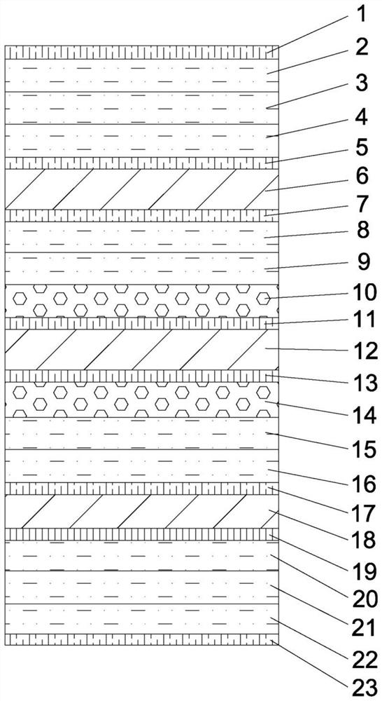
[0028] refer to figure 1 Shown:
[0029] A method for manufacturing a multilayer circuit board, comprising the steps of:
[0030] S1 Production of the first inner layer board: prepare the first inner layer board 6, the upper and lower ends of the first inner layer board 6 are electroplated, dry filmed and etched to form the first inner layer copper foil 5 and the second inner layer copper foil 7 respectively , the residual copper rate of the first inner layer copper foil 5 and the second inner layer copper foil 7 after etching is 56%;
[0031] S2 Production of the second inner layer board: prepare the second inner layer board 12, the upper and lower ends of the second inner layer board 12 are electroplated, dry filmed and etched to form the third inner layer copper foil 11 and the fourth inner layer copper foil 13 respectively , the residual copper rate of the third inner layer copper foil 11 after etching is 51%, and the residual copper rate of the fourth inner layer copper...
PUM
| Property | Measurement | Unit |
|---|---|---|
| Thickness | aaaaa | aaaaa |
| Thickness | aaaaa | aaaaa |
| Thickness | aaaaa | aaaaa |
Abstract
Description
Claims
Application Information