LED epitaxial wafer manufacturing method suitable for small-spacing display screen

An LED epitaxial wafer and manufacturing method technology, applied in electrical components, electric solid devices, circuits, etc., can solve problems such as the inability to meet the needs of small-pitch display applications, the shift of LED light-emitting wavelengths, and the rise of the ground state of quantum wells. Tucker effect, reduced wavelength blue shift, increased luminous intensity

Pending Publication Date: 2021-10-22
XIANGNENG HUALEI OPTOELECTRONICS
View PDF0 Cites 3 Cited by
  • Summary
  • Abstract
  • Description
  • Claims
  • Application Information

AI Technical Summary

Problems solved by technology

[0003] In the current LED quantum well growth method, the band gap of the material is limited, the ground state in the quantum well rises, and the luminous wavelength of the LED tends to shift to the short wavelength direction, that is, a blue shift occurs.
When different sizes of current are injected into the small-pitch display to change the luminous intensity, the blue shift of the LED light-emitting wavelength will be quite different, which cannot meet the application needs of small-pitch displays.

Method used


Image

  • LED epitaxial wafer manufacturing method suitable for small-spacing display screen
  • LED epitaxial wafer manufacturing method suitable for small-spacing display screen
  • LED epitaxial wafer manufacturing method suitable for small-spacing display screen

Examples


Embodiment 1

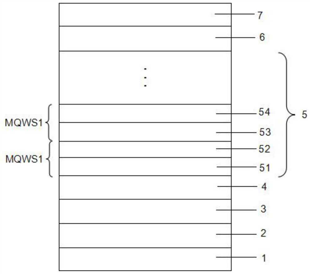
[0048] This embodiment adopts the LED epitaxial wafer manufacturing method suitable for small-pitch display screens provided by the present invention, adopts MOCVD to grow GaN-based LED epitaxial wafers, and uses high-purity H 2 or high purity N 2 or high purity H 2 and high purity N 2 The mixed gas as the carrier gas, high-purity NH 3 As the N source, the metal-organic source trimethylgallium (TMGa) is used as the gallium source, trimethylindium (TMIn) is used as the indium source, and the N-type dopant is silane (SiH 4 ), trimethylaluminum (TMAl) as the aluminum source, and the P-type dopant as magnesium dicene (CP 2 Mg), the reaction pressure is between 70mbar and 600mbar. The specific growth method is as follows (for the epitaxial structure, please refer to figure 1 ):

[0049] The method for manufacturing LED epitaxial wafers suitable for small-pitch display screens includes: processing a sapphire substrate 1, growing a low-temperature GaN buffer layer 2, growing a ...

Embodiment 2

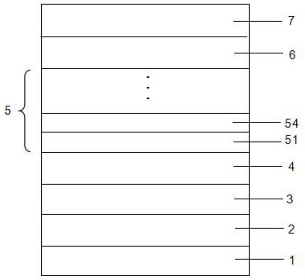
[0083] Comparative examples are provided below, that is, the growth method of the traditional LED epitaxial structure (for the epitaxial structure, please refer to figure 2 ).

[0084] Step 1: At a temperature of 1000-1100°C and a reaction chamber pressure of 100-300mbar, feed 100-130L / min of H 2 Under the conditions, process the sapphire substrate for 5-10 minutes.

[0085] Step 2: growing a low-temperature GaN buffer layer 2 and forming irregular small islands in the low-temperature GaN buffer layer 2 .

[0086] Specifically, the step 2 is further as follows:

[0087] At a temperature of 500-600°C and a reaction chamber pressure of 300-600mbar, 10000-20000sccm of NH is introduced 3 , 50-100sccm TMGa, 100-130L / min H 2 Under the condition of , growing the low-temperature GaN buffer layer 2 on the sapphire substrate 1, the thickness of the low-temperature GaN buffer layer 2 is 20-40nm;

[0088] At a temperature of 1000-1100°C and a reaction chamber pressure of 300-600mbar...


PUM

PropertyMeasurementUnit
thicknessaaaaaaaaaa
thicknessaaaaaaaaaa
thicknessaaaaaaaaaa

Abstract

The invention discloses an LED epitaxial wafer manufacturing method suitable for a small-spacing display screen. The method sequentially comprises the steps of: treating a substrate, growing a low-temperature GaN buffer layer, growing a non-doped GaN layer, growing a Si-doped N-type GaN layer, growing a multi-quantum well layer, growing an AlGaN electron blocking layer, growing a Mg-doped P-type GaN layer, and carrying out cooling. The step of growing the multi-quantum well layer sequentially comprises the steps of introducing a TMIn source, growing an MQWs1 and growing an MQWs2, the step of growing the MQWs1 comprises the steps of sequentially growing an InGaN well layer and an In<x>Al<y>Mg<1-x-y> layer, and the step of growing the MQWs2 comprises the steps of sequentially growing a GaO layer and a GaN barrier layer. The wavelength blue shift is reduced and the brightness of an LED is improved by adopting a novel LED epitaxial wafer manufacturing method, and the method is particularly suitable for manufacturing a small-spacing display screen.

Description

technical field [0001] The invention belongs to the technical field of LEDs, and in particular relates to a method for manufacturing LED epitaxial wafers suitable for small-pitch display screens. Background technique [0002] A light-emitting diode (Light-Emitting Diode, LED) is a semiconductor electronic device that converts electrical energy into light energy. When the LED has current flowing, the electrons and holes in the LED recombine in its multiple quantum wells to emit monochromatic light. As a new type of high-efficiency, environmentally friendly and green solid-state lighting source, LED is not only widely used as indoor and outdoor lighting, but also widely used in traffic lights, car lights, indoor and outdoor lighting and small-pitch display screens. [0003] In the current LED quantum well growth method, the band gap of the material is limited, the ground state in the quantum well rises, and the luminous wavelength of the LED tends to shift to the short wavele...

Claims


Application Information

Patent Timeline
Patent Type & Authority Applications(China)
IPC IPC(8): H01L33/00H01L33/06H01L27/15
CPCH01L33/007H01L33/06H01L27/156
Inventor 徐平
Owner XIANGNENG HUALEI OPTOELECTRONICS
Why Eureka
Try Eureka