SiC-based MIS device and preparation method thereof
A device, n-type technology, applied in the field of SiC-based MIS devices and their preparation, can solve problems such as poor repeatability of single crystals, achieve good gate control ability, improve the ability to withstand breakdown voltage, and alleviate excessive electric field concentration on the gate. The effect of the dielectric layer
- Summary
- Abstract
- Description
- Claims
- Application Information
AI Technical Summary
Problems solved by technology
Method used
Image
Examples
Embodiment 1
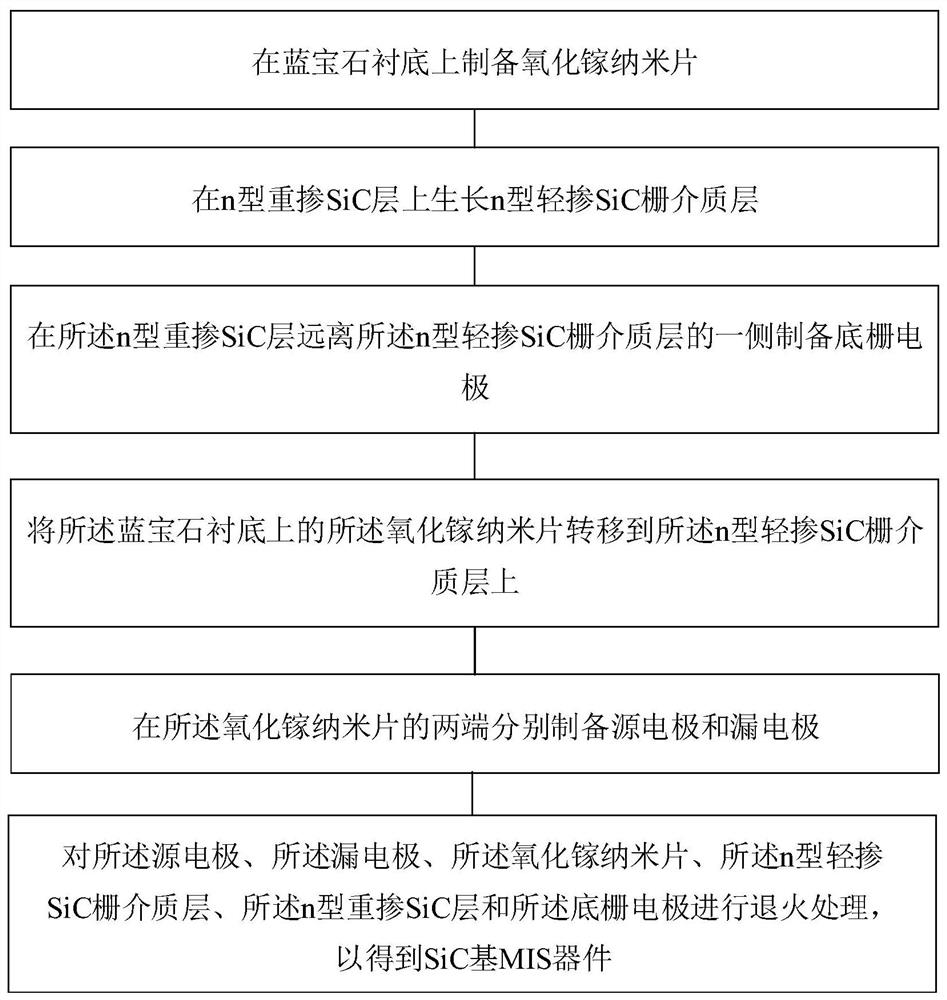
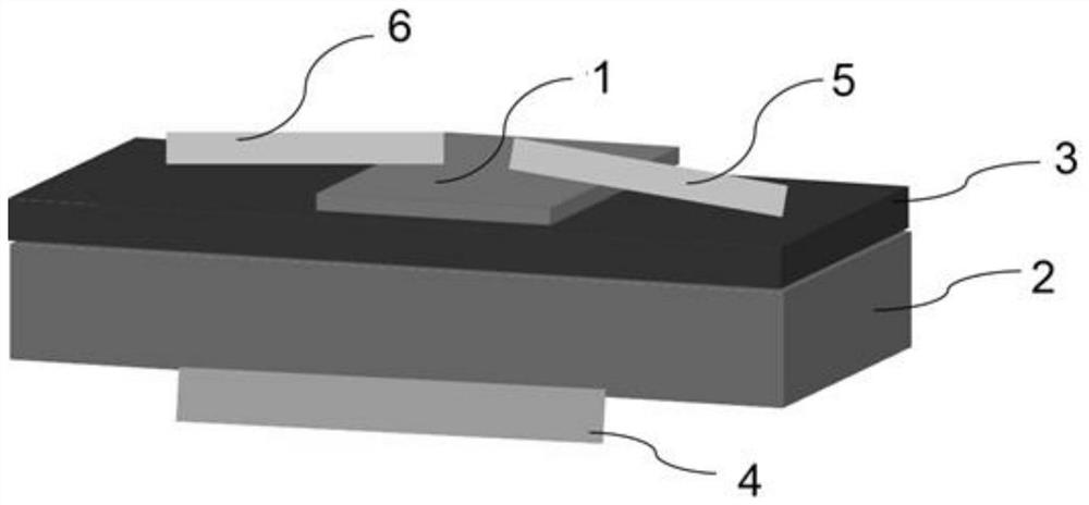
[0047] See figure 1 with figure 2 , figure 1 A schematic flow chart of a method for preparing a SiC-based MIS device provided by an embodiment of the present invention, figure 2 A schematic structural diagram of a SiC-based MIS device provided by an embodiment of the present invention. The invention provides a method for preparing a SiC-based MIS device, the method comprising the following steps:
[0048] Step 1, preparing gallium oxide nanosheets 1 on a sapphire substrate.
[0049] Step 1.1. Proportioning and uniformly mixing gallium oxide powder and carbon powder to prepare mixed powder.
[0050] Specifically, the gallium oxide powder and the carbon powder are mixed according to a mass ratio of 5:1, and put into a mortar for uniform grinding and mixing to prepare a mixed powder.
[0051] Step 1.2, using a chemical vapor deposition process to prepare gallium oxide nanosheets 1 on a sapphire substrate.
[0052] Specifically, the mixed powder was put into a corundum boa...
Embodiment 2
[0078] See figure 2 , this embodiment provides a SiC-based MIS device on the basis of the above-mentioned embodiments, and the SiC-based MIS device includes:
[0079] n-type heavily doped SiC layer 2;
[0080] The n-type lightly doped SiC gate dielectric layer 3 is located on the n-type heavily doped SiC layer 2;
[0081] Gallium oxide nanosheets 1 are located on the n-type lightly doped SiC gate dielectric layer 3;
[0082] The source electrode 5 and the drain electrode 6 are respectively located at both ends of the gallium oxide nanosheet 1;
[0083] The bottom gate electrode 4 is located on the side of the n-type heavily doped SiC layer 2 away from the n-type lightly doped SiC gate dielectric layer 3 .
[0084] In the description of the present invention, the terms "first" and "second" are only used for descriptive purposes, and cannot be understood as indicating or implying relative importance or implicitly specifying the quantity of indicated technical features. Thus...
PUM
| Property | Measurement | Unit |
|---|---|---|
| thickness | aaaaa | aaaaa |
| thickness | aaaaa | aaaaa |
| thickness | aaaaa | aaaaa |
Abstract
Description
Claims
Application Information


