Method for improving ultraviolet transmittance of aluminum nitride wafer
An aluminum nitride and transmittance technology is applied in the field of improving the ultraviolet transmittance of aluminum nitride wafers, which can solve the problems of poor diffusion effect and insignificant effect of the ultraviolet transmittance of the wafer, so as to ensure the output and improve the ultraviolet transmittance. Over-rate, high-yield effects
- Summary
- Abstract
- Description
- Claims
- Application Information
AI Technical Summary
Problems solved by technology
Method used
Image
Examples
Embodiment 1
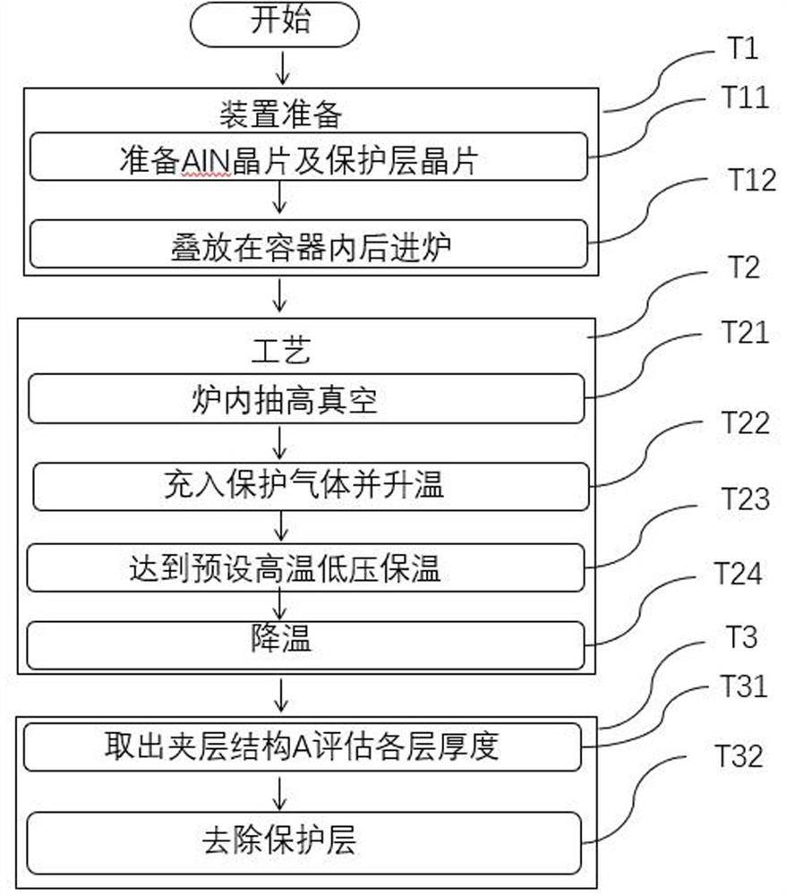
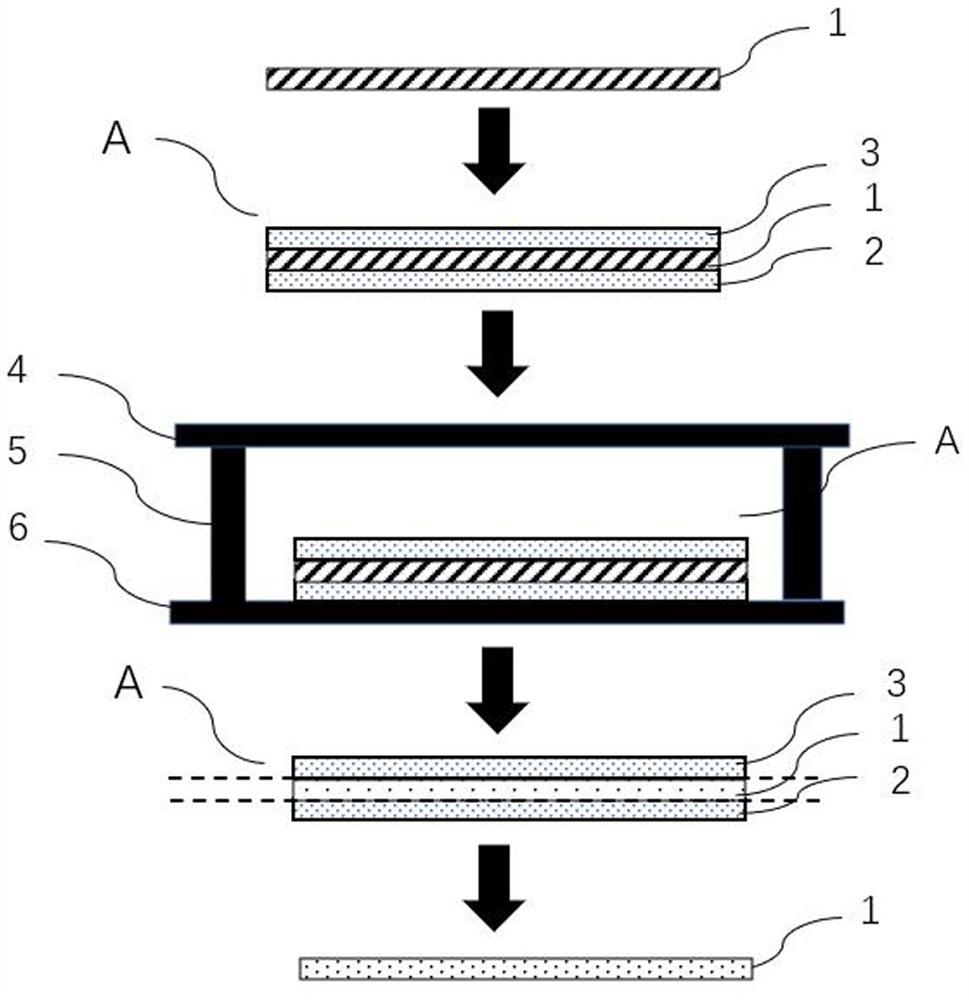
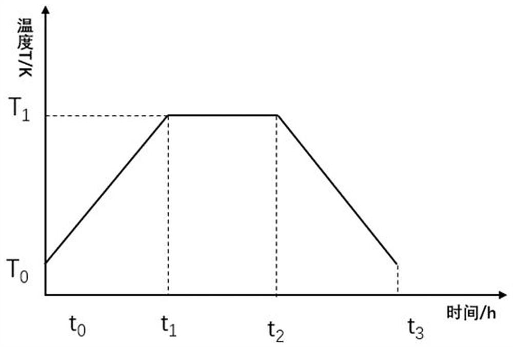
[0042] Reference attached Figure 1-3 and Figure 6 , the implementation steps of this illustrated embodiment are as follows:
[0043] Step T11: prepare an AlN single wafer 1 and two AlN polycrystalline protective layers 2 and 3, the orientation of the AlN single wafer 1 is c-direction, and its thickness is 0.6 mm, the thickness of the two AlN polycrystalline protective layers 2 and 3 Both are 1mm. Both the AlN single wafer and the two AlN polycrystalline protective layers were ground on both sides. The initial UV absorption coefficient of AlN single wafer is 30-45cm at 265nm wavelength -1 .
[0044] Step T12: The AlN single wafer and two AlN polycrystalline protective layers 2 and 3 form a sandwich composite structure A, and put the sandwich composite structure A into a container composed of upper and lower tungsten sheets 4, 6 and a cylindrical tungsten object 5, Form a closed environment. Place the assembled container in a high temperature furnace.
[0045]Step T21: ...
Embodiment 2
[0053] Reference attached figure 1 , 3 , 4-5 and Figure 7 , the implementation steps of this illustrated embodiment are as follows:
[0054] Step 1: Prepare multiple AlN single wafers 1 and multiple AlN polycrystalline protective layers 2, 3, 4, 5. The orientation of the AlN single wafer is c or m or r with an off angle, and its thickness is between 0.3- The thickness of the AlN polycrystalline protective layers 2, 3, 4 and 5 is between 0.5-4mm. Each single AlN wafer is fully covered by two AlN polycrystalline protective layers.
[0055] Step 2: Refer to attached Figure 4 Each AlN single chip 1 and its corresponding two AlN polycrystalline protective layers 2, 3, 4, 5 form a plurality of sandwich composite structures, and put the multiple sandwich composite structures into a multi-layer container to form a closed environment. Place the assembled container in a high temperature furnace.
[0056] Step 3: Vacuum the furnace to a vacuum degree of 10 -4 pa.
[0057] Step ...
Embodiment 3
[0063] Reference attached Figure 1-3 and Figure 6 , the implementation steps of this illustrated embodiment are as follows:
[0064] Step T11: prepare an AlN single wafer 1 and tantalum protective layers 2 and 3, the orientation of the AlN single wafer 1 is the m direction, double-sided grinding and its thickness is 2.2 mm, the thickness of the tantalum protective layers 2 and 3 are both 1.8 mm . AlN single wafers were carried out. The initial UV absorption coefficient of AlN single wafer is 45-55cm at 265nm wavelength -1 .
[0065] Step T12: AlN single wafer and tantalum sheet protection layers 2 and 3 form a sandwich composite structure A, and put the sandwich composite structure A into a container composed of upper and lower tantalum sheets 4, 6 and a cylindrical tungsten object 5 to form a closed environment . Place the assembled container in a high temperature furnace.
[0066] Step T21: evacuate the high-temperature furnace to a vacuum degree of 10 -5 pa.
[0...
PUM
| Property | Measurement | Unit |
|---|---|---|
| thickness | aaaaa | aaaaa |
| thickness | aaaaa | aaaaa |
| thickness | aaaaa | aaaaa |
Abstract
Description
Claims
Application Information


