

N-type boron nitride film/p-type monocrystalline silicon heterogeneous pn junction prototype device and preparation method thereof
A technology of boron nitride and single crystal silicon, applied in semiconductor/solid-state device manufacturing, semiconductor devices, electrical components, etc., can solve the problem of high-quality boron nitride thin film synthesis and effective doping limited, high-quality boron nitride thin film application Research on problems such as sluggishness and narrow boron nitride film growth window to overcome high intrinsic resistance, ease of industrialization, and improve growth quality and doping quality
- Summary
- Abstract
- Description
- Claims
- Application Information
AI Technical Summary
Problems solved by technology
Method used
Image

Examples
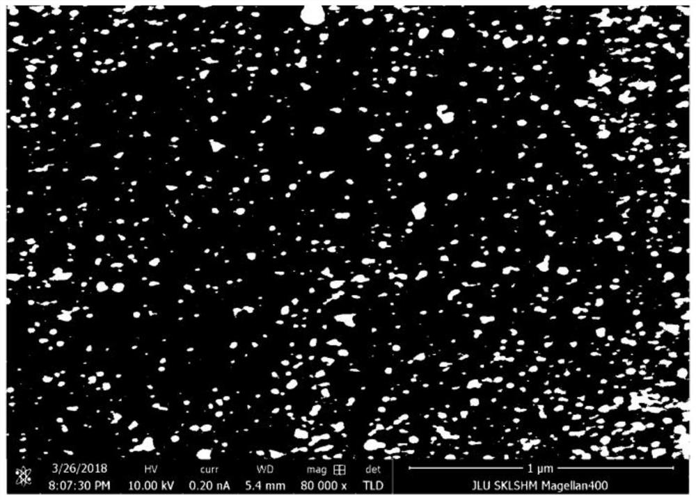
Embodiment 1
[0031] After the p-type silicon (100) single wafer cut according to the required size is ultrasonically cleaned in acetone, ethanol, and deionized water in sequence, it is dried with nitrogen and placed on the sample holder, and then sent to the vacuum deposition chamber. The vacuum degree in the deposition chamber is Draw up to 3×10 -5 Pa, heat the substrate to 500°C; continue vacuuming until the back vacuum of the deposition chamber reaches 3×10 -5 Pa, the reactive working gas argon 50sccm is introduced until the working pressure is 2Pa; the distance between the substrate and the target is 8cm, and the negative bias voltage of the substrate is -150V, and the sputtering power of the target is set to 150W before starting, and after pre-sputtering for 2 minutes, Remove the baffle and perform thin film sputtering for 2 hours to obtain n-type boron nitride thin film / p-type single crystal silicon heterogeneous pn junction. Prepare silver electrodes on both sides of the n-type bor...
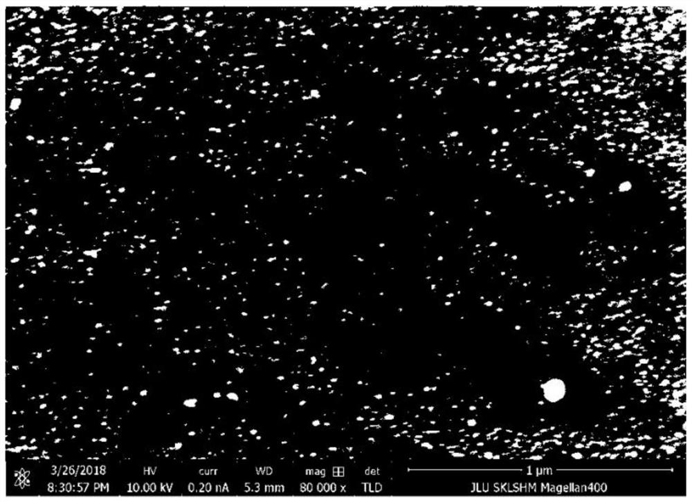
Embodiment 2
[0034] After the p-type silicon (100) single wafer cut according to the required size is ultrasonically cleaned in acetone, ethanol, and deionized water in sequence, it is dried with nitrogen and placed on the sample holder, and then sent to the vacuum deposition chamber. The vacuum degree in the deposition chamber is Draw up to 3×10 -5Pa, heat the substrate to 500°C; continue vacuuming until the back vacuum of the deposition chamber reaches 3×10 -5 At Pa, feed the reactive working gas Argon 50sccm and Nitrogen 20sccm until the working pressure is 2Pa; the distance between the substrate and the target is 8cm, add the substrate negative bias -150V, set the sputtering power of the target to 150W and start the sputtering, pre-sputtering After 2 minutes, the baffle was removed and film sputtering was performed for 2 hours to obtain n-type boron nitride film / p-type single crystal silicon heterogeneous pn junction. Silver electrodes are respectively prepared on both sides of the n-...
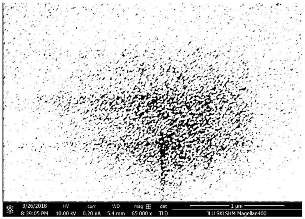
Embodiment 3
[0037] After the p-type silicon (100) single wafer cut according to the required size is ultrasonically cleaned in acetone, ethanol, and deionized water in sequence, it is dried with nitrogen and placed on the sample holder, and then sent to the vacuum deposition chamber. The vacuum degree in the deposition chamber is Draw up to 3×10 -5 Pa, heat the substrate to 500°C; continue vacuuming until the back vacuum of the deposition chamber reaches 3×10 -5 At Pa, feed the reactive working gas Argon 50sccm and Nitrogen 40sccm until the working pressure is 2Pa; the distance between the substrate and the target is 8cm, add the negative bias voltage of the substrate -150V, set the target sputtering power to 150W and start the sputtering, pre-sputtering After 2 minutes, the baffle was removed and film sputtering was performed for 2 hours to obtain n-type boron nitride film / p-type single crystal silicon heterogeneous pn junction. Silver electrodes are respectively prepared on both sides ...
PUM
| Property | Measurement | Unit |
|---|---|---|
| thickness | aaaaa | aaaaa |
| thickness | aaaaa | aaaaa |
Abstract
Description
Claims
Application Information