Preparation method for continuously growing tungsten selenide film through MOCVD

A tungsten selenide and thin film technology, applied in semiconductor/solid-state device manufacturing, electrical components, circuits, etc., can solve the problems of increasing selenium atom desorption, reducing nucleation density, reducing crystal quality, etc., to promote epitaxial growth, avoid Carbon pollution, effects of controlling nucleation density

Pending Publication Date: 2021-12-17
NANJING UNIV +1
View PDF0 Cites 0 Cited by
  • Summary
  • Abstract
  • Description
  • Claims
  • Application Information

AI Technical Summary

Problems solved by technology

[0003] So far, there are some obvious disadvantages in the previous MOCVD method to grow thin films, such as small crystal domain size (usually hundreds of nanometers); some MOCVD growth processes use carbon-containing MO precursors, such as (CH 3 ) 2 X or (C 2 h 5 ) 2 X, (X=S,Se), which inevitably leads to the deposition of carbon particles on the surface of TMDs; moreover, adopting a higher growth temperature reduces the nucleation density but also increases the desorption of Se atoms, leading to the Formation of vacancies, thereby reducing crystal quality

Method used


Image

  • Preparation method for continuously growing tungsten selenide film through MOCVD
  • Preparation method for continuously growing tungsten selenide film through MOCVD
  • Preparation method for continuously growing tungsten selenide film through MOCVD

Examples


Embodiment 1

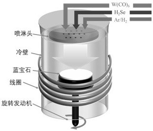
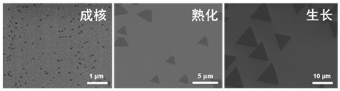
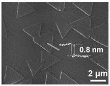
[0022] A method proposed in this embodiment uses MOCVD to continuously grow high-quality two-dimensional semiconductor thin films (WSe 2 ) preparation method, which comprises the following steps:

[0023] Step 1: cleaning the c-plane sapphire substrate;

[0024] Step 2: Put the cleaned substrate into the MOCVD reaction chamber, perform high-temperature pretreatment on the substrate, and then use tungsten hexacarbonyl (W(CO) 6 ) and hydrogen selenide (H 2 Se) is used as a precursor, and WSe is deposited on sapphire by continuous growth of MOCVD 2 film;

[0025] Step 3: WSe grown on sapphire 2 After the film is annealed, a continuous, large-area and high-quality crystalline finished product is obtained. Annealed at 400°C in hydrogen (H 2 ) and argon (Ar) mixed atmosphere for 2 hours, and the heating and cooling rate during the annealing process is 40°C / hour.

[0026] The specific process of step 1 is: immerse the sapphire substrate in acetone, sonicate it for 10 minutes, ...

Embodiment 2

[0033] A method proposed in this embodiment uses MOCVD to continuously grow high-quality two-dimensional semiconductor thin films (WSe 2 ) preparation method, which comprises the following steps:

[0034] Step 1: cleaning the c-plane sapphire substrate;

[0035] Step 2: Put the cleaned substrate into the MOCVD reaction chamber, perform high-temperature pretreatment on the substrate, and then use tungsten hexacarbonyl (W(CO) 6 ) and hydrogen selenide (H 2 Se) is used as a precursor, and WSe is deposited on sapphire by continuous growth of MOCVD 2 film;

[0036] Step 3: WSe grown on sapphire 2 After the film is annealed, a continuous, large-area and high-quality crystalline finished product is obtained. Annealed at 400°C in hydrogen (H 2 ) and argon (Ar) mixed atmosphere for 2 hours, and the heating and cooling rate during the annealing process is 40°C / hour.

[0037] The specific process of step 1 is as follows: immerse the sapphire substrate in acetone, ultrasonically tr...

Embodiment 3

[0044] A method proposed in this embodiment uses MOCVD to continuously grow high-quality two-dimensional semiconductor thin films (WSe 2 ) preparation method, which comprises the following steps:

[0045] Step 1: cleaning the c-plane sapphire substrate;

[0046] Step 2: Put the cleaned substrate into the MOCVD reaction chamber, perform high-temperature pretreatment on the substrate, and then use tungsten hexacarbonyl (W(CO) 6 ) and hydrogen selenide (H 2 Se) is used as a precursor, and WSe is deposited on sapphire by continuous growth of MOCVD 2 film;

[0047] Step 3: WSe grown on sapphire 2 After the film is annealed, a continuous, large-area and high-quality crystalline finished product is obtained. Annealed at 400°C in hydrogen (H 2 ) and argon (Ar) mixed atmosphere for 2 hours, and the heating and cooling rate during the annealing process is 40°C / hour.

[0048] The specific process of step 1 is as follows: immerse the sapphire substrate in acetone, ultrasonically tr...


PUM

PropertyMeasurementUnit
Thicknessaaaaaaaaaa

Abstract

The invention discloses a preparation method for continuously growing a two-dimensional semiconductor tungsten selenide (WSe2) film through MOCVD. The preparation method comprises the following steps: cleaning a c-plane sapphire substrate; putting the cleaned substrate into an MOCVD reaction cavity, carrying out high-temperature pretreatment on the substrate, and depositing a WSe2 thin film on sapphire through MOCVD continuous growth by taking tungsten hexacarbonyl (W(CO)6) and hydrogen selenide (H2Se) as precursors; and annealing the WSe2 film growing on the sapphire to obtain a continuous and large-area finished product with high crystallization quality. The film annealing is carried out in a mixed atmosphere of hydrogen (H2) and argon (Ar) at the temperature of 200-400 DEG C for 2-3 hours, and the heating and cooling rate in the annealing treatment process is 40-60 DEG C / h. The method has the advantages that gas sources are adopted as precursors, and carbon pollution of powder is avoided; and the continuous, large-area, high-electrical-performance and controllable-growth WSe2 thin film can be obtained after 60-100 min, and has important application prospects in the field of microelectronics.

Description

technical field [0001] The invention relates to a continuous MOCVD growth two-dimensional semiconductor tungsten selenide (WSe 2 ) film preparation method. Background technique [0002] Due to their unique electrical and optical properties, layered two-dimensional transition metal dichalcogenides (TMDs) materials have become important basic electronic materials for the continuation of Moore's Law in integrated circuits, thus triggering a research boom in next-generation nanoelectronic and optoelectronic devices. In order to obtain wafer-scale monolayer 2D TMDs with high crystalline quality, many scholars have tried many methods, including mechanical exfoliation of bulk TMD crystals, liquid phase exfoliation, chemical vapor deposition (CVD) and metal-organic chemical vapor deposition ( MOCVD) and so on. Compared with CVD, the MOCVD method can precisely control the growth parameters and precursor supply to grow wafer-sized films. This controllable deposition method is more ...

Claims


Application Information

Patent Timeline
IPC IPC(8): H01L21/02
CPCH01L21/02414H01L21/02568H01L21/0262H01L21/02664
Inventor 郝玉峰张建裕
Owner NANJING UNIV
Why Eureka
Try Eureka