High-sensitivity organic photodiode, array formed thereby and preparation method of high-sensitivity organic photodiode

A photodiode, high-sensitivity technology, applied in photovoltaic power generation, circuits, electrical components, etc., can solve the short-wave infrared organic photodiode noise and detection rate limitations, it is difficult to achieve high external quantum efficiency, exciton dissociation driving force reduction Small problems, to achieve the effects of trap-assisted recombination suppression, promotion of dark current and noise spectral density, and improvement of photosensitivity

Pending Publication Date: 2021-12-21
GUANGZHOU GUANGDA INNOVATION TECH CO LTD
View PDF0 Cites 1 Cited by
  • Summary
  • Abstract
  • Description
  • Claims
  • Application Information

AI Technical Summary

Problems solved by technology

However, such a low dark current density has not been reported for short-wave infrared organic photodiodes with spectral response in the near-infrared region or even beyond 1000 nm.
This is due to the fact that thermal excitation of charges begins to have a non-negligible effect on dark current as the energy gap of the material decreases, coupled with charge injection caused by pinholes and defects in the thin-film photoactive layer, making SWIR organic photodiodes inherently noisy and detection rate limit
In addition, the narrowing of the energy gap also reduces the driving force for exciton dissociation, making it difficult to achieve high external quantum efficiency.

Method used


Image

  • High-sensitivity organic photodiode, array formed thereby and preparation method of high-sensitivity organic photodiode
  • High-sensitivity organic photodiode, array formed thereby and preparation method of high-sensitivity organic photodiode
  • High-sensitivity organic photodiode, array formed thereby and preparation method of high-sensitivity organic photodiode

Examples


Embodiment 1

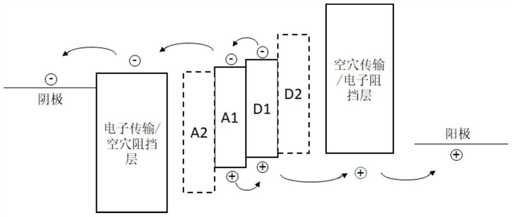
[0144] The device structure of the highly sensitive organic photodiode in this embodiment is as follows figure 1 As shown, from bottom to top are glass substrate (2mm), cathode (150nm), electron transport hole blocking layer (30nm), photosensitive layer (210nm), hole transport electron blocking layer (12nm), anode (150nm) and encapsulation layer.

[0145] Among them, the cathode is made of indium tin oxide (ITO); the electron transport hole blocking layer is made of zinc oxide (the carrier mobility in this material is ~10 -1 cm 2 V -1 S -1 ); the hole transport electron blocking layer is molybdenum oxide (the carrier mobility in this material is ~10 after testing -3 cm 2 V -1 S -1 ); the anode is metal silver; the encapsulation layer is epoxy resin.

[0146] The photosensitive layer adopts a ternary blended bulk heterojunction structure, which is a nanocrystalline structure. The donor material D1 is PTB7-Th, the acceptor material A1 is COTIC-4F, and the acceptor mat...

Embodiment 2

[0162] The device structure, materials used, and device preparation method in this embodiment are the same as those in Embodiment 1. The only difference is that the acceptor material A2 in Example 1 is replaced by IT-4F, and the mass ratio of D1:A1:A2 is 1:1.2:0.3.

[0163] The energy gap of the acceptor material A2, IT-4F, is calculated to be 1.48eV; its LUMO energy level is -4.14eV; the carrier mobility in this material is tested to be 3×10 -4 cm 2 V -1 S -1 .

[0164] The parameters of other identical materials used are the same as in Example 1.

Embodiment 3

[0166] The device structure, materials used, and device preparation method in this embodiment are the same as those in Embodiment 1. The only difference is that the acceptor material A2 in Example 1 is replaced by PC 71 BM, and the mass ratio of D1:A1:A2 is 1:1.2:0.3.

[0167] Acceptor material A2, PC 71 The energy gap of BM is calculated to be 2.13eV; its LUMO energy level is -4.20eV; the carrier mobility in the material is tested to be 6×10 -4 cm 2 V -1 S -1 ;

[0168] The parameters of other identical materials used are the same as in Example 1.


PUM

PropertyMeasurementUnit
thicknessaaaaaaaaaa
thicknessaaaaaaaaaa
sizeaaaaaaaaaa

Abstract

The invention relates to a high-sensitivity organic photodiode which comprises a photosensitive layer, wherein the photosensitive layer is of a bulk heterojunction structure, that is, (i) the photosensitive layer comprises a donor material D1 and an acceptor material A1; and donor materials D2-Dn, wherein the energy gap of the donor materials D2-Dn is larger than the energy gap of the donor material D1 and/or the energy gap of the acceptor material A1; or (ii)the photosensitive layer comprises a donor material D1 and an acceptor material A1; and acceptor materials A2-An, wherein the energy gap of the acceptor materials A2-An is larger than the energy gap of the donor material D1 and/or the energy gap of the acceptor material A1. Due to the addition of new components in the photosensitive layer, the defect state density of impurities in a bulk heterojunction energy gap is effectively reduced, a trap auxiliary composite channel of photogenerated charges is inhibited, the external quantum efficiency is enhanced, dark current is reduced, and the specific detection rate of the device is further improved. The invention also relates to an array formed by the same and a related preparation method.

Description

technical field [0001] The invention belongs to the field of organic photodetectors, and in particular relates to a high-sensitivity organic photodiode and an array thereof, and a preparation method of the organic photodiode. Background technique [0002] Organic photodiodes, and arrays made of them, are expected to be used in emerging fields such as machine vision, health monitoring, and biometric identification. However, although photodiodes based on silicon single crystals have been widely used as key components of image sensors, they still suffer from poor infrared response and complicated manufacturing processes, which lead to their high fabrication cost and limit its further application. Due to the thin photosensitive layer of the traditional front-incidence complementary metal oxide semiconductor (CMOS) image sensor, the near-infrared photoresponse efficiency drops rapidly at 700-1000nm. The external quantum efficiency (EQE) at the position is only 18% and 7% (refer...

Claims


Application Information

Patent Timeline
Patent Type & Authority Applications(China)
IPC IPC(8): H01L51/42H01L27/30H01L51/48
CPCH10K39/30H10K71/10H10K30/20Y02E10/549
Inventor 黄飞宋煜俞钢杨喜业邵麟
Owner GUANGZHOU GUANGDA INNOVATION TECH CO LTD
Why Eureka
Try Eureka