Array waveguide grating demultiplexer chip of cladding integrated micro lens and preparation method of array waveguide grating demultiplexer chip

A technology of arrayed waveguide grating and demultiplexer, which is applied in the direction of optical waveguide light guide, optical waveguide coupling, light guide, etc., can solve the problem of low photoelectric conversion efficiency, achieve the effects of convenient operation, reduced beam size, and improved efficiency

Pending Publication Date: 2022-01-07
HENAN SHIJIA PHOTONS TECH
View PDF3 Cites 1 Cited by
  • Summary
  • Abstract
  • Description
  • Claims
  • Application Information

AI Technical Summary

Problems solved by technology

[0005] Aiming at the technical problem of low photoelectric conversion efficiency when the existing arrayed waveguide grating demultiplexer chip is coupled with the detector in the vertical direction, the present invention proposes an arrayed waveguide grating demultiplexer with cladding integrated microlens Device chip and preparation method, the arrayed waveguide grating demultiplexer chip prepared by the preparation method of the present invention utilizes a semiconductor process to process a microlens on the cladding surface of the 45° total reflection optical path, and the microlens can realize the beam in the vertical direction Focusing and reducing the beam size, so that most of the beam energy can be received by the light receiving surface of the detector, improving the optical coupling efficiency

Method used


Image

  • Array waveguide grating demultiplexer chip of cladding integrated micro lens and preparation method of array waveguide grating demultiplexer chip
  • Array waveguide grating demultiplexer chip of cladding integrated micro lens and preparation method of array waveguide grating demultiplexer chip
  • Array waveguide grating demultiplexer chip of cladding integrated micro lens and preparation method of array waveguide grating demultiplexer chip

Examples


Embodiment 1

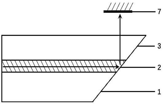
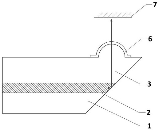
[0043] An arrayed waveguide grating demultiplexer chip with cladding integrated microlens, such as figure 2 As shown, it includes a sample layer 1, a core layer 2 and a cladding layer 3, the cladding layer 3 is located on the sample layer 1, the core layer 2 is located between the sample layer 1 and the cladding layer 3, and the top of the cladding layer 3 is etched with A microlens corresponding to the light beam passing through the core layer 2 . The output waveguide of the chip is provided with a total reflection angle, and the degree of the total reflection angle is 45°. The light beam in the core layer 2 corresponds to the center position of the microlens in the vertical direction after being reflected by the end face of the output waveguide. When the light beam propagates to the output waveguide along the horizontal direction in the core layer 2, it is reflected by the 45° total reflection angle at the output waveguide, and the light beam passes through the cladding 3 a...

Embodiment 2

[0047] A method for preparing an arrayed waveguide grating demultiplexer chip with cladding integrated microlenses, comprising the following steps:

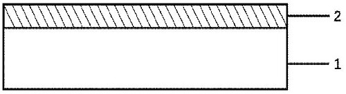
[0048] S1. Grow a germanium-doped silicon dioxide layer on the sample layer 1 prepared from silicon dioxide to obtain the core layer 2, and transfer the AWG demultiplexer waveguide pattern to the core layer by photolithography and etching processes 2 on. Specifically, as shown in Figure 3, a silicon dioxide sample is selected as the sample layer 1, and a core layer 2 of germanium-doped silicon dioxide with a thickness of 4 microns is grown on the surface of the sample layer 1 using PECVD equipment. The specific growth conditions It is: temperature 300°C, pressure 300mTorr, RF power 650W, SiH4 flow rate 15sccm, N2O flow rate 1500sccm, GeH4 flow rate 4sccm, deposition time 25min; use polysilicon as a mask, process arrayed waveguide grating by photolithography, etching and other processes The waveguide pattern of the user chip.

...


PUM

PropertyMeasurementUnit
angleaaaaaaaaaa
thicknessaaaaaaaaaa
reflectanceaaaaaaaaaa

Abstract

The invention provides an array waveguide grating demultiplexer chip of a cladding integrated micro lens and a preparation method of the array waveguide grating demultiplexer chip, and is used for solving the technical problem that the photoelectric conversion efficiency is low when an existing array waveguide grating demultiplexer chip is coupled with a detector in the vertical direction. According to the array waveguide grating demultiplexer chip prepared by the preparation method, a micro lens is processed on the surface of a cladding of a 45-degree total reflection light path by utilizing a semiconductor process, a light beam is horizontally propagated to an output waveguide in a core region layer, is reflected by a 45-degree total reflection angle at the output waveguide, and passes through the cladding in the vertical direction; and the micro-lens corresponding to the core area layer on the cladding is used for focusing, the size of the light beam is reduced, most of light beam energy of the light beam can be received by the light receiving surface of the detector, the optical coupling efficiency is improved, the distance between the chip and the detector does not need to be reduced due to the existence of the micro lens, the coupling distance between the chip and the detector is increased, the coupling packaging difficulty is reduced, and the efficiency is improved.

Description

technical field [0001] The invention relates to the technical field of an arrayed waveguide grating demultiplexer chip, in particular to an arrayed waveguide grating demultiplexer chip with a cladding integrated microlens and a preparation method thereof. Background technique [0002] With the rapid development of application markets such as big data, cloud computing, 5th generation mobile communications, the Internet of Things, and artificial intelligence, global data traffic growth has reached a compound annual growth rate of more than 25%. The rapid growth of data traffic puts forward more requirements on the performance of optical modules. Arrayed waveguide grating multiplexer and demultiplexer chips, namely AWG-shaped MUX and DEMUX chips, are important passive chips in high-speed optical modules. How to improve the coupling between optical passive chips and optical active chips (such as lasers and detectors) Efficiency is directly related to the performance parameters ...

Claims


Application Information

Patent Timeline
Patent Type & Authority Applications(China)
IPC IPC(8): G02B6/12G02B6/124G02B6/136G02B6/32G02B6/42
CPCG02B6/12009G02B6/124G02B6/136G02B6/32G02B6/4286G02B6/4204G02B2006/12102G02B2006/12176G02B2006/12197
Inventor 孙健苏晓华杨建周栗宝贵常夏森
Owner HENAN SHIJIA PHOTONS TECH
Why Eureka
Try Eureka