Silicon carbide semiconductor device and preparation method thereof

A technology of silicon carbide and semiconductor, which is applied in the direction of semiconductor devices, electrical components, circuits, etc. It can solve the problems of affecting the downward transmission of electrons and the increase of the on-resistance of power MOSFETs, so as to reduce the electric field intensity, reduce the resistance, and simplify the deposition process Effect

Pending Publication Date: 2022-01-25
SONGSHAN LAKE MATERIALS LAB +1
View PDF5 Cites 2 Cited by
  • Summary
  • Abstract
  • Description
  • Claims
  • Application Information

AI Technical Summary

Problems solved by technology

However, the depletion region formed by the P+ shielding region in the N-type drift region seriously affects the downward transmission of electrons, making the on-resistance of the power MOSFET larger

Method used


Image

  • Silicon carbide semiconductor device and preparation method thereof
  • Silicon carbide semiconductor device and preparation method thereof

Examples


Embodiment Construction

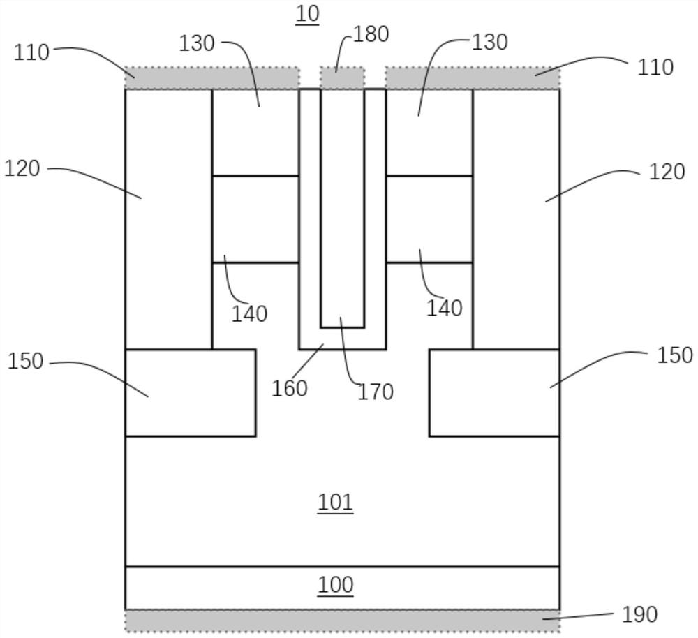
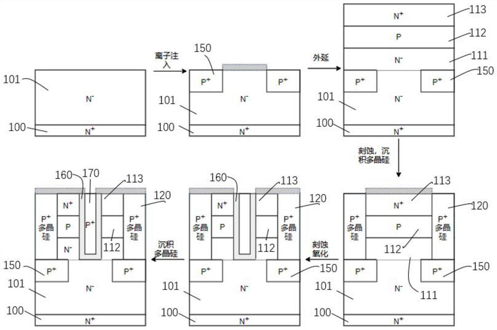
[0028] In order to facilitate the understanding of the present application, the present application will be described more fully below with reference to the relevant drawings. A preferred embodiment of the application is shown in the drawings. However, the present application can be implemented in many different forms and is not limited to the embodiments described herein. On the contrary, the purpose of providing these embodiments is to make the disclosure of this application more thorough and comprehensive.

[0029] Unless otherwise defined, all technical and scientific terms used herein have the same meaning as commonly understood by one of ordinary skill in the technical field to which this application belongs. The terms used herein in the specification of the application are only for the purpose of describing specific embodiments, and are not intended to limit the application. As used herein, the term "and / or" includes any and all combinations of one or more of the asso...


PUM

PropertyMeasurementUnit
thicknessaaaaaaaaaa
thicknessaaaaaaaaaa
thicknessaaaaaaaaaa

Abstract

The invention relates to a silicon carbide semiconductor device and a preparation method thereof. Two sides of a trench gate dielectric layer are respectively provided with two heavily doped polycrystalline silicon trench regions of a second conductive type. Due to the energy band structure of silicon carbide and polycrystalline silicon, the area of a depletion region of a shielding region is reduced by the polycrystalline silicon trench region. The reduction of the area of the depletion region not only can reduce the electric field intensity at the corner of the protective trench gate medium, but also can slightly hinder electron flow, thereby reducing the resistance of the drift region. The polycrystalline silicon deposition process of the second conduction type is relatively simple, and the problems of depth and transverse diffusion caused by the traditional silicon carbide ion implantation process of the second conduction type are avoided by adopting the heavily doped polycrystalline silicon trench region of the second conduction type.

Description

technical field [0001] The present application relates to the field of power semiconductor devices, in particular to a silicon carbide semiconductor device and a preparation method. Background technique [0002] A power metal-oxide-semiconductor field-effect transistor (MOSFET) is a widely used semiconductor transistor that can be used as a switching device in high-power device applications. A power MOSFET has three electrodes, including a source and drain separated by a channel, and a gate near the channel. Power MOSFETs can be turned on or off by applying a bias voltage to the gate. When a power MOSFET is turned on (that is, in the "on state"), current is conducted through the channel between the source and drain. When the power MOSFET is off, no current flows in the channel. In addition, power MOSFETs are unipolar devices, and current conduction is carried by majority carriers, so power MOSFETs have very high switching speeds. However, the drift region of the power MO...

Claims


Application Information

Patent Timeline
Patent Type & Authority Applications(China)
IPC IPC(8): H01L29/06H01L29/10H01L29/66H01L29/78
CPCH01L29/0615H01L29/1079H01L29/78H01L29/66477
Inventor 陈昭铭殷鸿杰罗惠馨夏经华张安平
Owner SONGSHAN LAKE MATERIALS LAB
Why Eureka
Try Eureka