Preparation method for growing germanium sulfide single crystal film on SiO2 substrate

A technology of single crystal thin film and germanium sulfide, which is applied in semiconductor/solid-state device manufacturing, gaseous chemical plating, final product manufacturing, etc., can solve the problems of long growth time, unfavorable processing and preparation of devices, etc., to reduce the growth temperature and promote The effect of cryolysis

Pending Publication Date: 2022-01-25
SOUTH CHINA UNIV OF TECH
View PDF0 Cites 3 Cited by
  • Summary
  • Abstract
  • Description
  • Claims
  • Application Information

AI Technical Summary

Problems solved by technology

This method requires a long growth time, and the obtained crystals are l

Method used


Image

  • Preparation method for growing germanium sulfide single crystal film on SiO2 substrate
  • Preparation method for growing germanium sulfide single crystal film on SiO2 substrate
  • Preparation method for growing germanium sulfide single crystal film on SiO2 substrate

Examples


Embodiment

[0037] The SiO provided in this example 2 The preparation method for growing a germanium sulfide single crystal film on a substrate can obtain a high-quality germanium sulfide single crystal film with a thickness of about 1 micron on an amorphous substrate. The prepared single crystal thin film has good crystal quality, flat surface and roughness of only a few tenths of a nanometer. After the photoluminescence spectrum test, there are two luminescence peaks at the wavelengths of 410nm and 445nm in the blue-violet light band, indicating that it has the potential to be used in the field of visible light detection.

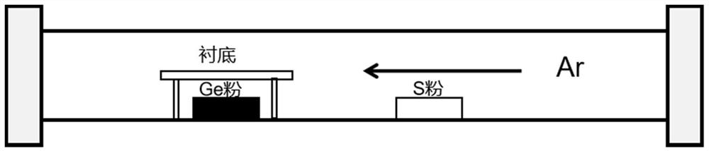
[0038] This embodiment provides a SiO 2 A preparation method for growing a germanium sulfide single crystal thin film on a substrate, comprising the following steps:

[0039] (1) Preferably, the substrate is Si / SiO with a p-(100) crystal orientation and a thickness of 300nm 2 substrate.

[0040] (2) Clean the surface of the substrate with acetone, ethanol and dei...


PUM


Abstract

The invention discloses a preparation method for growing a germanium sulfide single crystal film on a SiO2 substrate. The method comprises the following steps: cleaning the surface of the substrate by using acetone, ethanol and deionized water, wherein the substrate material is a Si/SiO2 substrate or a SiO2 glass substrate; carrying out photoetching on the substrate, spin-coating photoresist, and after photoetching is carried out, obtaining a groove pattern through dry etching or wet etching; depositing a layer of germanium crystal in the groove pattern of the substrate to obtain a processed substrate; and placing the processed substrate in chemical vapor deposition equipment for growth, taking high-purity sulfur powder and high-purity germanium powder as growth sources, and then preparing the germanium sulfide single crystal thin film on the SiO2 substrate. The preparation method provided by the invention is simple to operate, the monocrystal germanium sulfide GeS2 can be grown on the SiO2 substrate, and the monocrystal germanium sulfide crystal is high in quality and small in surface roughness and has a forbidden band width corresponding to blue-violet light of a visible light band.

Description

technical field [0001] The invention relates to the technical field of wide bandgap photodetection semiconductor material growth, in particular to a SiO 2 A preparation method for growing a germanium sulfide single crystal thin film on a substrate. Background technique [0002] Germanium sulfide (GeS 2 ) is a layered in-plane anisotropic Group IV chalcogenide semiconductor with high bandgap width. Its crystal structure is a monoclinic structure. combined. Due to this unique in-plane anisotropic structure, germanium sulfide has unique properties such as photoelectric anisotropy and electrophase transition, and has been widely used in polarized light detectors, memristors, optical memories, and high-energy batteries. At present, the commonly used method for germanium sulfide crystal growth is chemical vapor transport (CVT): high-purity sulfur powder and high-purity germanium powder are melted and sealed in a quartz tube according to a certain ratio, and grown at 1000 ° C fo...

Claims


Application Information

Patent Timeline
IPC IPC(8): H01L31/18H01L21/02H01L31/032H01L31/0392C23C16/30C23C16/513
CPCH01L31/18H01L31/0392H01L31/032H01L21/02422H01L21/0242H01L21/0243H01L21/02568H01L21/0262C23C16/305C23C16/513Y02P70/50
Inventor 李国强陈胜王文樑柴吉星
Owner SOUTH CHINA UNIV OF TECH
Why Eureka
Try Eureka