

Target material for semiconductor industry and preparation method thereof
An industrial and semiconductor technology, applied in metal material coating process, ion implantation plating, coating, etc., can solve problems such as poor strength performance and poor target density.
- Summary
- Abstract
- Description
- Claims
- Application Information
AI Technical Summary
Problems solved by technology
Method used
Image

Examples
preparation example Construction
[0043] The preparation method of described modified bentonite dispersant is:
[0044] S1: Put the bentonite into the hydrochloric acid solution with a mass fraction of 10-20% for stirring and dispersing treatment, the stirring speed is 100-500r / min, the stirring time is 10-20min, after the stirring is completed, wash with water, dry and set aside;
[0045] S2: Put the bentonite in S1 into a calcination furnace for calcination, the calcination temperature is 400-600°C, the calcination time is 10-20min, and then the calcination temperature is reduced to 200°C at a rate of 1-3°C / min, and continue Keep warm for 20-30min, and finally cool down to room temperature naturally;
[0046]S3: send the bentonite of S2 into a grinder for grinding, the grinding speed is 1000-1500r / min, the grinding time is 10-20min, and the grinding is completed to obtain the bentonite dispersant;
[0047] S4: Send the bentonite dispersant into the refiner for stirring treatment, the treatment speed is 500-...
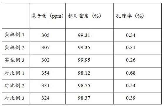
Embodiment 1
[0072] A kind of target material for semiconductor industry in this embodiment includes the following raw materials in parts by weight:
[0073] 10 parts of germanium, 5 parts of tellurium, 4 parts of selenium, 1 part of modified bentonite dispersant, 1 part of modifier, 1 part of rare earth agent modified graphite powder, 30 parts of silicon powder;
[0074] The preparation method of described modified bentonite dispersant is:
[0075] S1: Put the bentonite into the hydrochloric acid solution with a mass fraction of 10% for stirring and dispersing treatment, the stirring speed is 100r / min, the stirring time is 10min, after the stirring is completed, wash with water, dry, and set aside;
[0076] S2: Put the bentonite in S1 into a calcination furnace for calcination. The calcination temperature is 400°C, and the calcination time is 10 minutes. Then, the calcination temperature is reduced to 200°C at a rate of 1°C / min, and the heat preservation is continued for 20 minutes, and f...
Embodiment 2
[0100] A kind of target material for semiconductor industry in this embodiment includes the following raw materials in parts by weight:
[0101] 20 parts of germanium, 10 parts of tellurium, 10 parts of selenium, 2 parts of modified bentonite dispersant, 6 parts of modifier, 3 parts of rare earth agent modified graphite powder, 40 parts of silicon powder;
[0102] The preparation method of described modified bentonite dispersant is:
[0103] S1: Put the bentonite into the hydrochloric acid solution with a mass fraction of 20% for stirring and dispersing treatment, the stirring speed is 500r / min, the stirring time is 20min, after the stirring is completed, wash with water, dry, and set aside;
[0104] S2: Put the bentonite in S1 into a calcination furnace for calcination, the calcination temperature is 600°C, the calcination time is 20min, then reduce the calcination temperature to 200°C at a rate of 3°C / min, continue to keep warm for 30min, and finally cool naturally to room te...
PUM
 Abstract
Description
Claims
Application Information