Se microtube/bromine-lead-cesium heterojunction and preparation method and photoelectric application thereof
A micron-tube, bromine-lead-cesium technology, applied in the field of Se microtube/bromide-lead-cesium heterojunction and its preparation, can solve the problems of limiting two-dimensional heterojunction research, complex stability, problems, etc., and achieve excellent photoelectric performance , long effective carrier lifetime, and high trap state density
- Summary
- Abstract
- Description
- Claims
- Application Information
AI Technical Summary
Problems solved by technology
Method used
Image

Examples
Embodiment 1
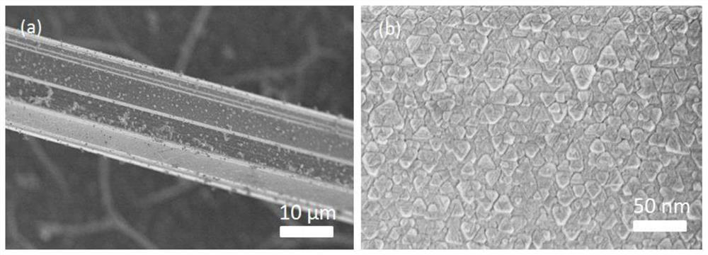
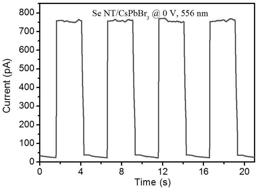
[0024] Example 1: Preparation of SE Micron Tubes / CSPBBRs of 1D-2D P-N Structure 3 Triangular heterojunction
[0025] In the horizontal tubular furnace, high-purity argon (99.99%) as the carrier gas, first take the appropriate amount of SE powder in a clean quartz booon, will be placed in the level of SE powder into the constant temperature of the horizontal tube furnace Area. Then, the acetone, alcohol, deionized water was then cleaned, and the silicon-blown silicon-blown wafer was vertically placed in the quartz tube, and the quartz boat responded to 22cm. The growth temperature is 380 ° C, the growth time is 6 h, and the argon flow is 200cm. 3 / min, after the reaction is completed, stop heating, naturally fell to room temperature, to obtain a large number of SE micron tubes on the silicon wafer. High purity argon (99.999%) as carrier gas, high purity PBBR powder (99.999%) and CSBR 2 (99.999%) As the reactive source placement tubular furnace, a clean flexible polyester fiber s...
Embodiment 2
[0026] Example 2: Preparation of SE Micron Tubes / CSPBBR of 1D-1D P-N Structure 3 Nano-line heterojunction
[0027] In the horizontal tubular furnace, high-purity argon (99.99%) as the carrier gas, first take the appropriate amount of SE powder in a clean quartz booon, will be placed in the level of SE powder into the constant temperature of the horizontal tube furnace Area. Then, the acetone, alcohol, deionized water was then cleaned, and the silicon-blown silicon-blown wafer was vertically placed in the quartz tube, and the quartz boat responded to 22cm. The growth temperature is 380 ° C, the growth time is 6 h, and the argon flow is 200cm. 3 / min, after the reaction is completed, stop heating, naturally fell to room temperature, to obtain a large number of SE micron tubes on the silicon wafer. High purity argon (99.999%) as carrier gas, high purity PBBR powder (99.999%) and CSBR 2 (99.999%) As the reactive source placement tubular furnace, a clean flexible polyester fiber sub...
Embodiment 3
[0028] Example 3: Preparation of 1D-2D P-N Structure SE Micron Tube / CSPBBR3 Square heterojunction
[0029] In the horizontal tubular furnace, high-purity argon (99.99%) as the carrier gas, first take the appropriate amount of SE powder in a clean quartz booon, will be placed in the level of SE powder into the constant temperature of the horizontal tube furnace Area. Then, the acetone, alcohol, deionized water was then cleaned, and the silicon-blown silicon-blown wafer was vertically placed in the quartz tube, and the quartz boat responded to 22cm. The growth temperature is 380 ° C, the growth time is 6 h, and the argon flow is 200cm. 3 / min, after the reaction is completed, stop heating, naturally fell to room temperature, to obtain a large number of SE micron tubes on the silicon wafer. High purity argon (99.999%) as carrier gas, high purity PBBR powder (99.999%) and CSBR 2 (99.999%) As the reactive source placement tubular furnace, a clean flexible polyester fiber substrate c...
PUM
 Abstract
Description
Claims
Application Information
 - R&D
- Intellectual Property
- Life Sciences
- Materials
- Tech Scout
- Unparalleled Data Quality
- Higher Quality Content
- 60% Fewer Hallucinations
Browse by: Latest US Patents, China's latest patents, Technical Efficacy Thesaurus, Application Domain, Technology Topic, Popular Technical Reports.
© 2025 PatSnap. All rights reserved.Legal|Privacy policy|Modern Slavery Act Transparency Statement|Sitemap|About US| Contact US: help@patsnap.com