Annealing method for reducing indium arsenide surface dot number

An indium arsenide and indium arsenide single crystal technology is applied in chemical instruments and methods, self-solidification methods, chemical reactive gases, etc. The effect of reducing the number of pips, reducing the number of pips

Pending Publication Date: 2022-03-25
广东先导微电子科技有限公司
View PDF8 Cites 0 Cited by
  • Summary
  • Abstract
  • Description
  • Claims
  • Application Information

AI Technical Summary

Problems solved by technology

However, there is currently no annealing method for reducing the number of dots on the surface of indium arsenide.

Method used


Image

  • Annealing method for reducing indium arsenide surface dot number

Examples


Embodiment 1

[0027] (1) The non-doped indium arsenide crystal grown by the VGF method is cut into a single wafer with a size of 3 inches by multi-wire cutting, and a clean indium arsenide single crystal wafer is obtained after edging, cleaning and drying.

[0028] (2) Clean the quartz tube and the quartz sample holder in ultrasonic for 10 hours in hydrofluoric acid, then rinse them with deionized water for 10 minutes, put them in a drying oven to dry after rinsing.

[0029] (3) Place the indium arsenide single crystal wafers in an orderly and spaced manner vertically on a clean quartz sample holder, and then place the quartz sample holder horizontally in the quartz tube.

[0030] (4) Vacuum the quartz tube, when its vacuum degree is less than or equal to 10 -3 Pa, sintering and sealing with hydrogen-oxygen flame.

[0031] (5) Put the sealed quartz tube into a horizontal annealing furnace for annealing, which includes heating, constant temperature and cooling stages. When the temperature ...

Embodiment 2

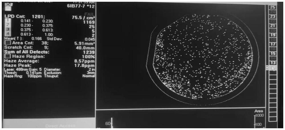
[0033] (1) The non-doped indium arsenide crystal grown by the VGF method is cut into a single wafer with a size of 2 inches by multi-wire cutting, and a clean indium arsenide single crystal wafer is obtained after edging, cleaning and drying.

[0034] (2) The quartz tube and the quartz sample holder were ultrasonically cleaned in aqua regia for 10 hours, then rinsed with deionized water for 10 minutes, and then placed in a drying oven for drying.

[0035] (3) Place the indium arsenide single crystal wafers in an orderly and spaced manner vertically on a clean quartz sample holder, and then place the quartz sample holder horizontally in the quartz tube.

[0036] (4) Vacuum the quartz tube, when its vacuum degree is less than or equal to 10 -3 Pa, sintering and sealing with hydrogen-oxygen flame.

[0037] (5) Put the sealed quartz tube into a horizontal annealing furnace for annealing, which includes heating, constant temperature and cooling stages. When the temperature rises ...

Embodiment 3

[0039] (1) The non-doped indium arsenide crystal grown by the VGF method is obtained by multi-wire cutting to obtain a single wafer with a size of 4 inches. After grinding, cleaning and drying, a clean indium arsenide single crystal wafer is obtained.

[0040] (2) Clean the quartz tube and the quartz sample holder in ultrasonic for 10 hours in hydrofluoric acid, then rinse them with deionized water for 10 minutes, put them in a drying oven to dry after rinsing.

[0041] (3) Place the indium arsenide single crystal wafers in an orderly and spaced manner vertically on a clean quartz sample holder, and then place the quartz sample holder horizontally in the quartz tube.

[0042] (4) Vacuum the quartz tube, when its vacuum degree is less than or equal to 10 -3 Pa, sintering and sealing with hydrogen-oxygen flame.

[0043] (5) Put the sealed quartz tube into a horizontal annealing furnace for annealing, which includes heating, constant temperature and cooling stages. When the tem...


PUM


Abstract

The invention belongs to the technical field of semiconductor material processing, and discloses an annealing method for reducing the number of indium arsenide surface dots. The method comprises the following steps: performing multi-line cutting on indium arsenide crystals to obtain single crystal wafers, performing edge grinding, cleaning and drying to obtain clean indium arsenide single crystal wafers, then sequentially and vertically placing the clean indium arsenide single crystal wafers on a cleaned and dried quartz sample rack at intervals, and then horizontally placing the quartz sample rack in a quartz tube; the quartz tube is sintered and sealed after being vacuumized, then the quartz tube is put into a horizontal annealing furnace to be annealed, the annealing process comprises the stages of temperature rise, constant temperature and temperature reduction, the temperature rise stage refers to that the room temperature is raised to 840-856 DEG C, the constant temperature stage refers to that the temperature is kept at 840-856 DEG C for 30-60 hours, and the temperature reduction stage refers to that the quartz tube is cooled to the room temperature. The method can effectively reduce or eliminate the residual stress on the surface of indium arsenide and reduce the number of dots on the surface of the wafer.

Description

technical field [0001] The invention belongs to the technical field of semiconductor material processing, and in particular relates to an annealing method for reducing the number of dots on the surface of indium arsenide. Background technique [0002] Indium arsenide is a narrow bandgap III-V compound semiconductor material. As a substrate material, it can grow heterojunction materials such as InAsSb / InAsPSb and is widely used in infrared light-emitting devices; it can also grow AlGaSb superlattice structure and is widely used For mid-infrared quantum cascade lasers. Therefore, indium arsenide is widely used in gas monitoring, low-loss optical fiber communication and other fields. [0003] As a single crystal substrate, InAs material needs to have low dislocation density, good lattice integrity, suitable electrical parameters and high uniformity. The current crystal growth method of indium arsenide is mainly the vertical gradient condensation method (Vertical gradient cond...

Claims


Application Information

Patent Timeline
IPC IPC(8): C30B29/40C30B33/02C30B11/00C30B25/18
CPCC30B29/40C30B33/02C30B11/00C30B25/186Y02P70/50
Inventor 唐林锋宋向荣马金峰周铁军刘火阳廖和杰
Owner 广东先导微电子科技有限公司
Why Eureka
Try Eureka