Supercharge Your Innovation With Domain-Expert AI Agents!

Integrated Schottky VDMOS device with optimized on-resistance

A technology of on-resistance and Schottky contact, which is applied in the direction of semiconductor devices, electrical components, circuits, etc., can solve the problems of weakened forward conduction performance and increased cell width, so as to improve switching speed and reverse recovery ability , Reduce switching loss, increase the effect of on-resistance

Active Publication Date: 2022-04-05
UNIV OF ELECTRONICS SCI & TECH OF CHINA
View PDF10 Cites 0 Cited by
  • Summary
  • Abstract
  • Description
  • Claims
  • Application Information

AI Technical Summary

Problems solved by technology

[0005] The technical problem to be solved by the present invention is to provide an integrated Schottky VDMOS device structure with optimized on-resistance for the problem that the increase in the cell width of the common source integrated Schottky device leads to the weakening of the forward conduction performance.

Method used


Image

  • Integrated Schottky VDMOS device with optimized on-resistance
  • Integrated Schottky VDMOS device with optimized on-resistance
  • Integrated Schottky VDMOS device with optimized on-resistance

Examples


Embodiment Construction

[0030] The principles and characteristics of the present invention will be described below in conjunction with specific embodiments and accompanying drawings. The examples given are only used to explain the present invention and are not intended to limit the scope of the present invention.

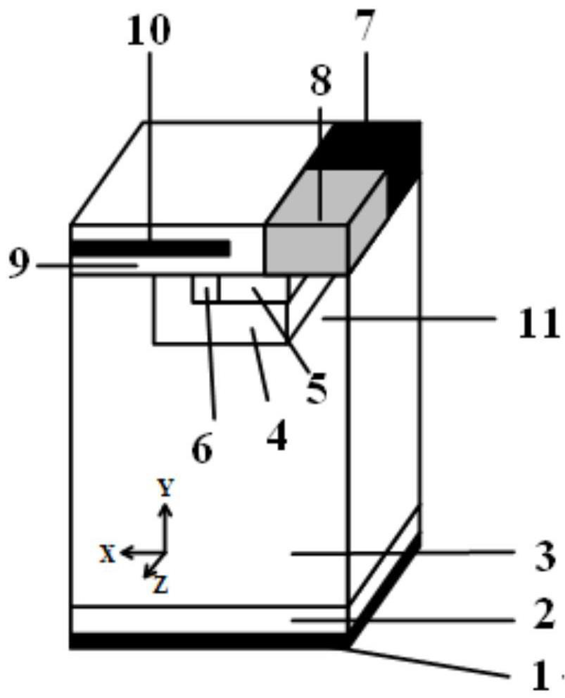
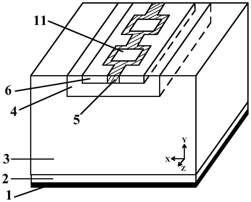
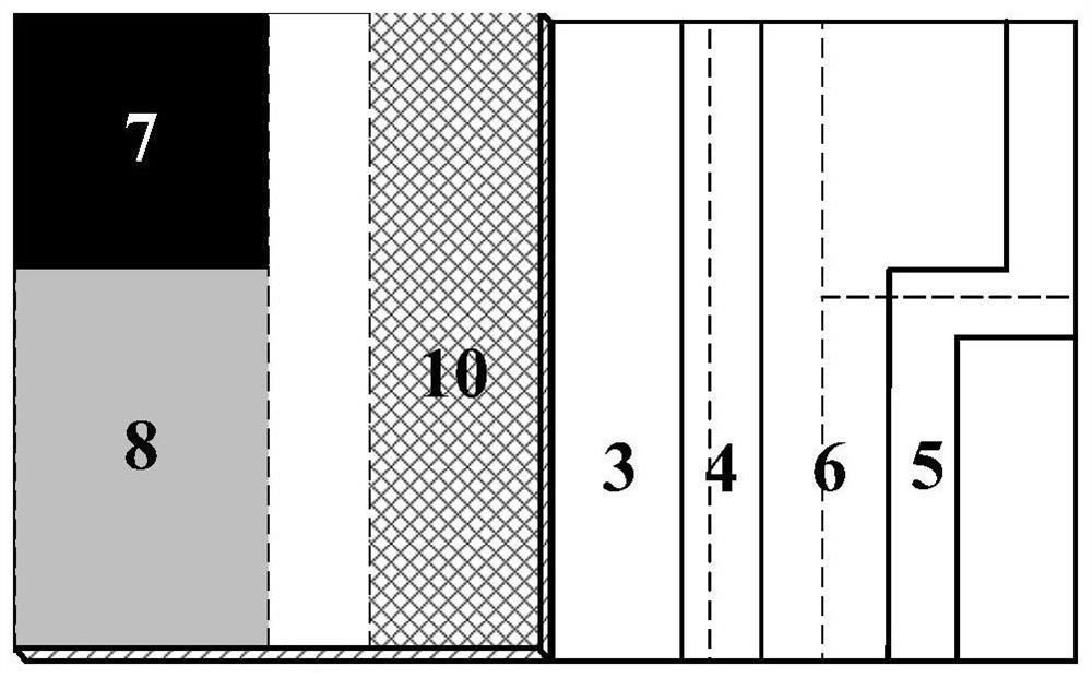
[0031] This embodiment provides an integrated Schottky VDMOS device with optimized on-resistance, including a metal drain electrode 1 arranged in sequence from bottom to top, an N-type semiconductor substrate 2, and an N-type epitaxial layer 3; Schottky contact electrode 8 above the epitaxial layer 3, source ohmic contact electrode 7 behind the Schottky contact electrode 8;

[0032] The direction from the N-type semiconductor substrate 2 to the N-type epitaxial layer 3 is the Y-axis direction; the direction from the source ohmic contact electrode 7 to the Schottky contact electrode 8 is the Z-axis direction, and the X-axis is perpendicular to the Y-axis and Z axis;

[0033] The integrated...


PUM

PropertyMeasurementUnit
thicknessaaaaaaaaaa
thicknessaaaaaaaaaa
electrical resistanceaaaaaaaaaa

Abstract

The invention relates to an integrated Schottky VDMOS device for optimizing on-resistance, and belongs to the technical field of power semiconductors. According to the invention, a mode of forming holes in the P-type well region for multiple times in the longitudinal direction and integrating Schottky contact is adopted, the transverse area of device cells is not increased, the forward conduction capability of the device is basically consistent with that of a traditional structure, and meanwhile, Schottky contact is utilized to provide a current path for reverse recovery so as to reduce the reverse recovery charge of a body diode and improve the reliability of the device. And the reverse recovery process is accelerated. The integrated Schottky VDMOS structure for optimizing the on-resistance has better switching characteristic and reverse recovery capability, and meanwhile, the static characteristic of the device is basically consistent with that of a traditional structure.

Description

technical field [0001] The invention belongs to the technical field of power semiconductors, in particular to an integrated Schottky VDMOS device with optimized on-resistance. Background technique [0002] Since the 1950s, power semiconductor devices have played a very important role in electronic control circuits and power switching circuits. Among them, power MOSFET devices are widely used in the power semiconductor device market due to their low on-resistance and high switching speed. [0003] Vertical double-diffused metal-oxide-semiconductor field effect transistor (Vertical Double-Diffused Metal Oxide Semiconductor, VDMOSFET) is a type of device often used in power MOSFETs, mainly used in automotive electronics, frequency converters, switching power supplies, motor speed controllers, field of high frequency oscillators. [0004] In many high-power switching applications, the power MOSFET requires a freewheeling diode to provide a current path when the MOSFET is turne...

Claims


Application Information

Patent Timeline
Patent Type & Authority Applications(China)
IPC IPC(8): H01L29/06H01L29/78
Inventor 张有润贺鹏陈航欧阳钢陈劭桦张波
Owner UNIV OF ELECTRONICS SCI & TECH OF CHINA
Features
  • R&D
  • Intellectual Property
  • Life Sciences
  • Materials
  • Tech Scout
  • Unparalleled Data Quality
  • Higher Quality Content
  • 60% Fewer Hallucinations
Learn More