Etching composition and application thereof

A composition and etching technology, applied in the direction of surface etching compositions, semiconductor devices, chemical instruments and methods, etc., can solve the problems of bumps prone to side etching, incomplete and uneven etching, etc., and achieve circuit or solder joints. Good morphology, no damage or small damage, good etching uniformity

Pending Publication Date: 2022-04-12
SHANGHAI PHICHEM MATERIAL CO LTD
View PDF0 Cites 3 Cited by
  • Summary
  • Abstract
  • Description
  • Claims
  • Application Information

AI Technical Summary

Problems solved by technology

[0004] 1. Bumps are prone to side erosion due to isotropic etching;
[0005] 2. The seed layer is prone to undercut (undercut);
[0006] 3. Aluminum electrode damage problem;
[0007] 4. Incomplete and uneven etching caused by bubbles formed during the etching chemical reaction
These corrosions will have a fatal blow to the reliability of the chip

Method used


Image

  • Etching composition and application thereof
  • Etching composition and application thereof
  • Etching composition and application thereof

Examples


preparation example Construction

[0055] The preparation method of the etching composition in the present invention can be any one known to those skilled in the art, such as physical blending.

[0056] The present invention also provides the application of the above etching composition, which is used for manufacturing display devices; further, the etching composition is used for making bumps on chips.

[0057] The chip of the present invention includes a bump and a seed layer under the bump; the bump includes an upper layer made of tin or tin alloy, and a lower layer made of nickel or nickel-copper alloy. The types of tin alloys mentioned in this application are not particularly limited, and generally refer to alloys composed of tin and copper, silver, lead and other metals. In some embodiments, an electroplating layer is further included between the bumps and the seed layer.

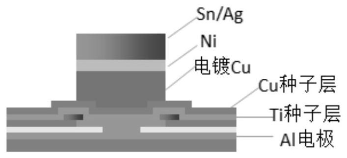
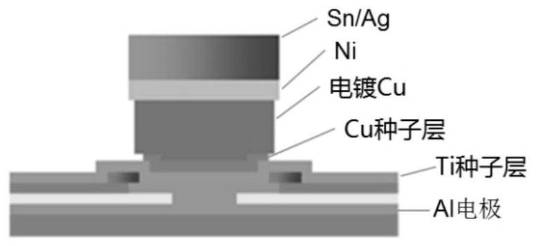
[0058] Such as figure 1 As shown, it is a schematic diagram of a chip bump, wherein the chip includes a bump and a seed layer below ...

Embodiment

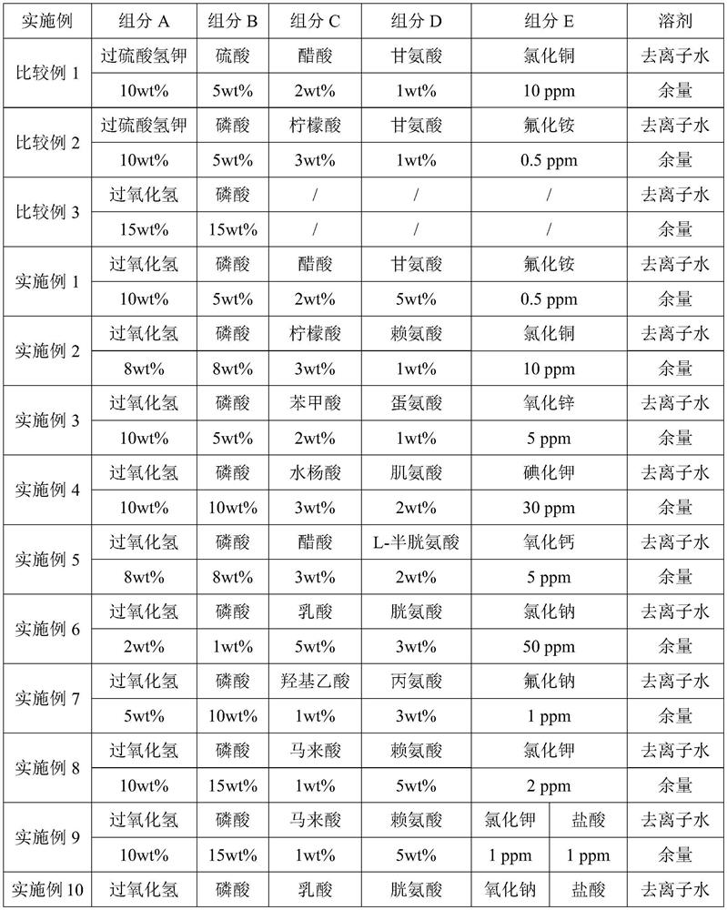
[0061] The technical solutions of the present invention are described in detail below through examples, but the protection scope of the present invention is not limited to the examples. Unless otherwise specified, the raw materials in the present invention are all commercially available.

[0062] The performance parameter test index of etching composition of the present invention:

[0063] 1. The amount of side etching CD loss, such as Figure 1~2 As shown, the shrinkage of electroplated copper in the horizontal direction before and after copper etching is called side etching loss (CD loss), and the unit is μm. After corrosion, electroplated copper and copper seed layer should be as flush as possible with the Ni or Sn / Ag layer. Shrinkage, so low CD is the best performance value, and the general application requirement is less than 1μm.

[0064] 2. The amount of undercut undercut, such as Figure 1~2 As shown, on one side of the bump, the amount of shrinkage of the copper se...


PUM


Abstract

The invention discloses an etching composition, which comprises a component A: 1-30 wt% of an oxidant, a component B: 0.5-20 wt% of an inorganic acid, a component C: 0-15 wt% of an organic acid, a component D: 0.01-15 wt% of a chelating agent, a component E: 0-0.1 wt% of an ionic compound and/or other inorganic acids except the inorganic acid of the component B, and deionized water. The invention also provides an application of the etching composition in manufacturing a chip. The chip comprises a salient point and a seed layer below the salient point. Each bump comprises an upper layer made of tin or tin alloy and a lower layer made of nickel or nickel-copper alloy.

Description

technical field [0001] The invention relates to the technical field of chip processing, in particular to an etching composition and application thereof. Background technique [0002] In the integrated circuit manufacturing process, it is often necessary to define extremely fine patterns (Pattern) on the wafer. The main way to form these patterns is to use etching (Etching) technology to produce micro-lithography (Micro-lithography) The photoresist pattern is transferred to the material under the photoresist to form the complex architecture of the collective circuit. After the chip is manufactured, a special packaging factory will make solder joints or bumps for the wafer, with the purpose of building an interconnection medium for the next step of interconnection of a single chip. We call this process Advanced Packaging Process. Similarly, the packaging factory will also rearrange the wiring or make bumps for the interconnection of the chip through a graphical process. Aft...

Claims


Application Information

Patent Timeline
Patent Type & Authority Applications(China)
IPC IPC(8): C23F1/44C23F1/18
CPCC09K13/08C09K13/06C23F1/18H01L24/11H01L2224/11C09K13/10C09K13/04H01L21/32134C09K13/00C23F1/16C23F1/44
Inventor 高晓义胡杭剑
Owner SHANGHAI PHICHEM MATERIAL CO LTD
Why Eureka
Try Eureka