Preparation method of microwave thin film integrated circuit
A microwave thin film and integrated circuit technology, applied in the manufacture of circuits, electrical components, semiconductors/solid devices, etc., can solve the problems of copper etching layer corrosion penetration, reduce circuit adhesion, process limitations, etc., to overcome circuit adhesion , broaden the applicability, the effect of wide applicability
- Summary
- Abstract
- Description
- Claims
- Application Information
AI Technical Summary
Problems solved by technology
Method used
Image
Examples
preparation example Construction
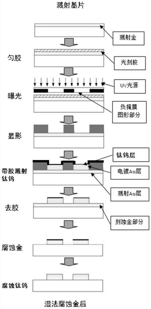
[0058] The invention provides a method for preparing a microwave thin film integrated circuit, comprising the following steps:
[0059] S1. Carry out metallization treatment on the surface of the ceramic substrate to form a metal composite film layer;
[0060] In the metal composite film layer, the bottom layer is in contact with the surface of the ceramic substrate, and the surface layer is away from the ceramic substrate;
[0061] The surface layer of the metal composite film layer is an Au film layer;
[0062] S2. Attach photoresist on the surface of the metal composite film layer, and remove the photoresist in the circuit pattern area to expose the metal composite film layer in the circuit pattern area, and keep the photoresist in the non-circuit pattern area;
[0063] S3, electroplate the circuit board obtained in step S2, and form a gold-plated layer on the surface of the metal composite film layer exposed in the circuit pattern area;
[0064] S4. Carry out vacuum sput...
Embodiment 1
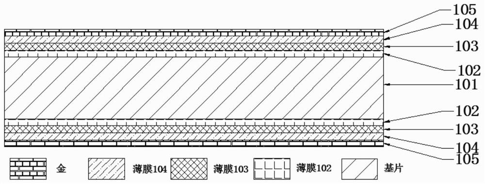
[0118] S1, with polishing 99 alumina as ceramic substrate 101 (thickness is 0.381mm), first remove the pollutant on the surface of ceramic substrate 101 with cleaning agent, then, utilize vacuum sputtering again on the surface of ceramic substrate 101 (comprising the front and the back) sequentially form a TaN layer-TiW layer-Ni layer-Au layer to obtain a metal composite film layer.
[0119] see figure 2 , wherein 101 is a ceramic substrate, 102-105 are metal composite film layers, 102 is a TaN layer, 103 is a TiW layer, 104 is a Ni layer, and 105 is an Au layer. In 102 to 105, the thickness of each layer is 0.3 μm.
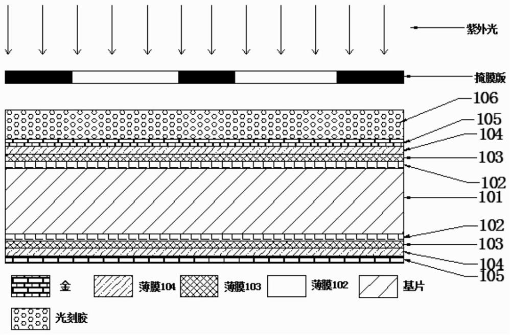
[0120] S2, with AZP4620 type positive photoresist: the solution of acetone=1mL: 10mL is photoresist solution, this photoresist solution is sprayed on the metal composite film layer surface of ceramic substrate front, spray glue temperature is 85 ℃, spray The flow rate of the glue is 1.2mL / min, the number of times of glue spraying is 4 times, and then baked at ...
Embodiment 2
[0129] S1-S3: same as embodiment 1. Afterwards, the obtained circuit board was placed in an environment with a humidity of 75% and a temperature of 28° C. for 10 minutes.
[0130] S4, electroplating with glue: specifically operate according to step S4 in embodiment 1, the result is as follows Figure 10 as shown, Figure 10 It is a schematic structural diagram of the circuit after step S4 in Example 2; wherein, 109 is the part of gold infiltration, that is, the infiltration and plating phenomenon has occurred.
[0131] S5, sputtering anti-etching TiW mask protective layer 108: specifically operate according to step S5 in Example 1, the result is as follows Figure 11 as shown, Figure 11 It is a schematic structural diagram of the circuit processed in step S5 in embodiment 2. It can be seen that the anti-etching TiW mask protection layer is not formed in the non-pattern area, and there is no mask layer on the surface of the gold-infiltrated part; it can be seen that the pr...
PUM
| Property | Measurement | Unit |
|---|---|---|
| Thickness | aaaaa | aaaaa |
| Thickness | aaaaa | aaaaa |
| Thickness | aaaaa | aaaaa |
Abstract
Description
Claims
Application Information
 - R&D Engineer
- R&D Manager
- IP Professional
- Industry Leading Data Capabilities
- Powerful AI technology
- Patent DNA Extraction
Browse by: Latest US Patents, China's latest patents, Technical Efficacy Thesaurus, Application Domain, Technology Topic, Popular Technical Reports.
© 2024 PatSnap. All rights reserved.Legal|Privacy policy|Modern Slavery Act Transparency Statement|Sitemap|About US| Contact US: help@patsnap.com


