Printed circuit board and method of manufacturing the same

A printed circuit board and circuit layer technology, applied in the direction of printed circuit manufacturing, printed circuit, printed circuit, etc., can solve the problems of limiting and reducing the line width and spacing of circuit patterns

Pending Publication Date: 2022-04-19
SAMSUNG ELECTRO MECHANICS CO LTD
View PDF1 Cites 0 Cited by
  • Summary
  • Abstract
  • Description
  • Claims
  • Application Information

AI Technical Summary

Problems solved by technology

However, such a plating process is limited in reducing the line width and space of the circuit pattern as required due to the process margin of the exposure process and the isotropic etching process (wet etching process)

Method used


Image

  • Printed circuit board and method of manufacturing the same
  • Printed circuit board and method of manufacturing the same
  • Printed circuit board and method of manufacturing the same

Examples


Embodiment Construction

[0029] Hereinafter, embodiments of the present disclosure will be described as follows with reference to the accompanying drawings.

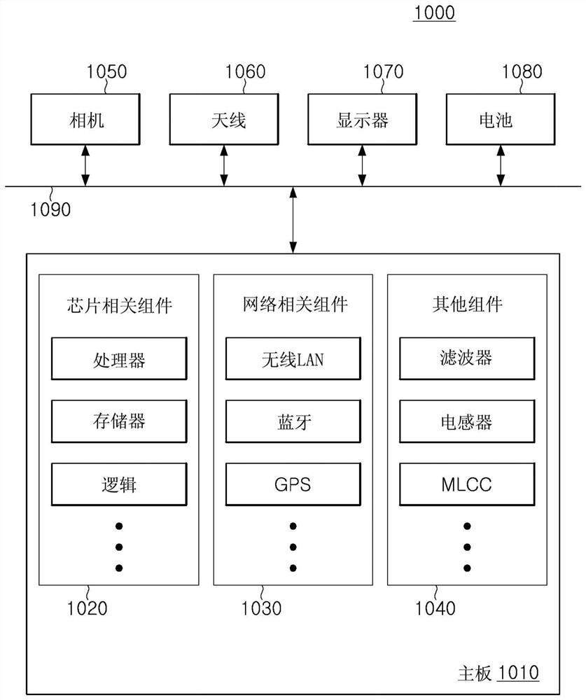
[0030] figure 1 is a schematic block diagram illustrating an example of an electronic device system.

[0031] refer to figure 1 , the electronic device 1000 may accommodate the motherboard 1010 therein. The motherboard 1010 may include chip-related components 1020 , network-related components 1030 , other components 1040 , etc., physically or electrically connected thereto. These components may be connected to other components that will be described below through various signal lines 1090 .

[0032] Chip-related components 1020 may include: memory chips, such as volatile memory (eg, dynamic random access memory (DRAM)), non-volatile memory (eg, read-only memory (ROM)), flash memory, etc.; application processors Chips, such as central processing units (e.g., central processing units (CPUs)), graphics processors (e.g., graphics processing unit...


PUM


Abstract

The invention provides a printed circuit board and a method of manufacturing the same. The printed circuit board includes an insulating layer and a circuit layer disposed on the insulating layer. The circuit layer includes a first circuit pattern and a second circuit pattern. Each of the first circuit pattern and the second circuit pattern has a first side surface, a second side surface opposite to the first side surface, and a top surface connected to an end of the first side surface and an end of the second side surface when viewed from a cross section. The first side surface of the first circuit pattern and the first side surface of the second circuit pattern face each other. A height of the first side surface of the first circuit pattern is greater than a height of the second side surface of the first circuit pattern, and a height of the first side surface of the second circuit pattern is greater than a height of the second side surface of the second circuit pattern.

Description

[0001] This application claims the benefit of priority of Korean Patent Application No. 10-2020-0133219 filed on October 15, 2020 at the Korean Intellectual Property Office, the entire disclosure of which is hereby incorporated by reference. technical field [0002] The present disclosure relates to a printed circuit board and a method of manufacturing the printed circuit board. Background technique [0003] Recently, high-density printed circuit boards (PCBs) are required in the electronic component industry to support 5G high-speed communications and artificial intelligence (AI). Microcircuit technology is important for high-density PCBs, and research and development are currently underway to reduce line widths and spaces of circuit patterns. [0004] Common circuit formation methods implemented in the field of PCB design are semi-additive process (SAP), modified SAP (MSAP), sealing holes (TT), and the like. However, such a plating process is limited in reducing the line ...

Claims


Application Information

Patent Timeline
Patent Type & Authority Applications(China)
IPC IPC(8): H05K1/11H05K3/40
CPCH05K1/116H05K3/4038H05K2201/095H05K3/4644H05K2203/308H05K3/08H05K2203/095H05K2201/098H05K2203/072H05K2201/09736H01L23/49822H01L23/49811H05K3/4623H05K1/115H05K1/09H05K3/06H05K1/181H05K1/0296H05K1/11
Inventor 李栽欣张容蕣
Owner SAMSUNG ELECTRO MECHANICS CO LTD
Why Eureka
Try Eureka