Perovskite thin film, precursor composition thereof, preparation method and semiconductor element

A composition, perovskite technology, applied in the fields of semiconductor devices, semiconductor/solid-state device manufacturing, oxide/hydroxide preparation, etc., can solve the problem of high surface roughness, affecting component performance, and difficult to precisely control the uniformity of film formation And film quality and other issues, to achieve the effect of large lattice arrangement, reduced impurities, high component efficiency and stability

Pending Publication Date: 2022-04-22
IND TECH RES INST
View PDF0 Cites 3 Cited by
  • Summary
  • Abstract
  • Description
  • Claims
  • Application Information

AI Technical Summary

Problems solved by technology

[0003] The current perovskite thin film preparation technology is prepared by chemical solution deposition method, but the existing technology has the problem of high surface roughness when forming a large-area film, and it is difficult to accurately control the uniformity and thickness of the film. The quality of the film, which in turn affects the performance of the components made of it

Method used


Image

  • Perovskite thin film, precursor composition thereof, preparation method and semiconductor element
  • Perovskite thin film, precursor composition thereof, preparation method and semiconductor element
  • Perovskite thin film, precursor composition thereof, preparation method and semiconductor element

Examples


preparation example Construction

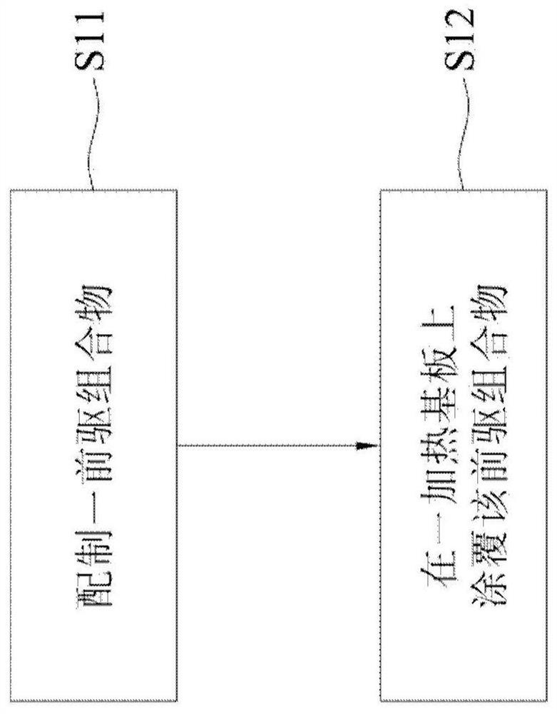
[0064] In the process flow of the preparation method disclosed in the present disclosure, the coating method in the coating step includes slit coating, doctor blade coating, air knife coating or inkjet coating.

[0065] The doctor blade coating is suitable for industrial-scale production, and its film-forming principle is to make nucleation and crystal growth proceed simultaneously by controlling the solvent evaporation rate at high temperature. Therefore, the perovskite film produced by the present disclosure also has a larger grain size and a smoother film surface than those produced by other processes.

[0066] In a specific embodiment, the operating temperature of the knife coating is 130 to 180° C., and the speed of the knife coating is 1 to 50 mm / s; in other embodiments, the operating temperature of the knife coating can be 140, 150, 160 or 170°C, but not limited thereto.

[0067] The preparation method of the perovskite thin film of the present disclosure may further i...

Embodiment 1-1

[0114] Preparation of the precursor composition: γ-butyrolactone and dimethyl sulfoxide are used as the mixed solvent of the precursor composition; the perovskite precursor salt of the precursor composition includes formamidine hydroiodide (FAI), lead bromide (PbBr 2 ), methylamine hydrobromide (MABr), lead iodide (PbI 2 ), cesium iodide (CsI).

[0115] First, formamidine hydroiodide (FAI), lead bromide (PbBr 2 ), methylamine hydrobromide (MABr), lead iodide (PbI 2 ), cesium iodide (CsI) and other perovskite precursor salts are sequentially dispersed or dissolved to form the first solution, wherein the volume molar concentration of the formamidine hydriodide is 0.159M, and the volume molar concentration of the lead bromide is 0.159M, the volume molar concentration of the methylamine hydrobromide is 0.159M, the volume molar concentration of the lead iodide is 0.9M and the volume molar concentration of the cesium iodide is 1.35M; the gamma-butyrolactone and di The volume rat...

Embodiment 1-2 to 1-3

[0126] Examples 1-2 to 1-3: Preparation of perovskite thin films

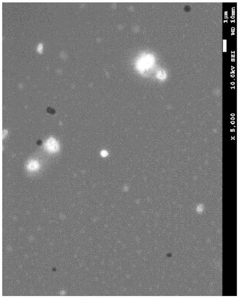
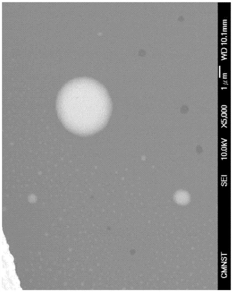
[0127] The preparation method of its perovskite film is the same as that of Example 1-1, when the volume molar concentration of 18-crown-6 in its precursor composition is changed to 0.25mM and 0.45mM respectively; The surface observation and crystallinity analysis of the titanium ore thin film were carried out and recorded in image 3 , Figure 4 , Figure 5B , Figure 5C , Figure 6A and Figure 6B .


PUM

PropertyMeasurementUnit
sizeaaaaaaaaaa
sizeaaaaaaaaaa
sizeaaaaaaaaaa

Abstract

A perovskite thin film includes crystal grains having a crystal structure represented by [A], [B], [X], [C], and n as defined in the specification, the crystal grains being represented by [A], [B], [X], [C], and n. The invention also provides a precursor composition for preparing the perovskite thin film, a preparation method of the perovskite thin film and a semiconductor element comprising the thin film. The perovskite thin film prepared by the invention has the effect of effectively reducing the surface roughness due to the optimal lattice arrangement, even if a large-area film is formed, a semiconductor element of the perovskite thin film can also realize high element efficiency and stability, and the perovskite thin film has an application prospect.

Description

technical field [0001] The present disclosure relates to a material used for a photoelectric conversion element, in particular to a thin film with a perovskite structure, a method for making the same, a precursor composition thereof, and a semiconductor element using the same. Background technique [0002] With the vigorous development of material science and processing technology, perovskite-type materials have been widely used in recent years due to their advantages such as high light absorption capacity, adjustable band gap, high defect tolerance, good carrier mobility and solution processability. It has attracted much attention in the application fields of semiconductor components such as light-emitting diodes, lasers, and light-emitting transistors. [0003] The current perovskite thin film preparation technology is prepared by chemical solution deposition method, but the existing technology has the problem of high surface roughness when forming a large-area film, and i...

Claims


Application Information

Patent Timeline
Patent Type & Authority Applications(China)
IPC IPC(8): H01L51/42H01L51/44H01L51/48H01L51/46
CPCH10K71/00H10K85/00H10K30/10H10K30/80C01B13/18Y02E10/549H10K30/151
Inventor 黄国玮童永樑邱荣宾邱培庭吴世雄
Owner IND TECH RES INST
Why Eureka
Try Eureka