

Method for rapidly preparing (100) single crystal copper
A single crystal copper, rapid technology, applied in the direction of single crystal growth, single crystal growth, chemical instruments and methods, etc., can solve the problems of complexity, large thermal damage, low quality of single crystal, etc., to reduce process temperature, thermal damage Small, the effect of reducing process time
- Summary
- Abstract
- Description
- Claims
- Application Information
AI Technical Summary
Problems solved by technology
Method used
Image

Examples
Embodiment 1
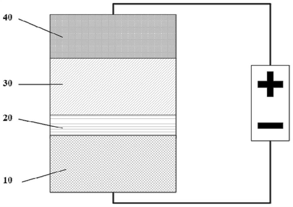
[0050] like image 3 Shown, a kind of fast preparation method of (100) single-crystal copper of the present invention can be realized by following specific processing steps:
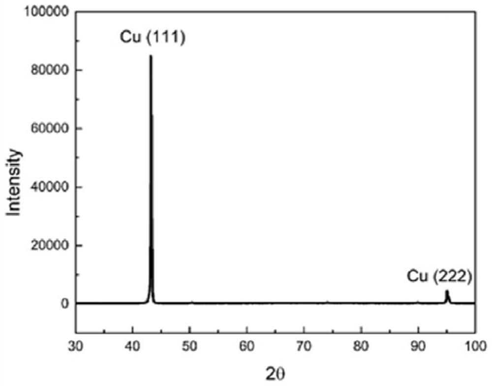
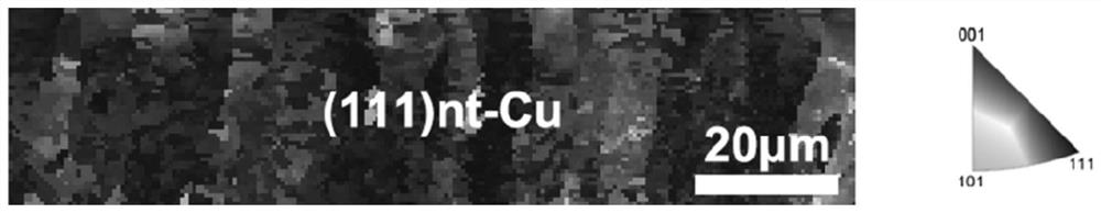
[0051] Step 1: provide a nano-twinned Cu 20 (such as figure 1 and figure 2 As shown), it has a high-density twin boundary, the grains are columnar and have a (111) preferred orientation, and the average diameter of the columnar grains is 8 μm. The nano-twinned Cu is prepared on the substrate 10 by direct current or pulse electroplating, and the substrate is rolled polycrystalline Cu. The thickness of the nano-twinned Cu is 30 μm.
[0052] Step 2: Using the nano-twinned Cu described in Step 1 as a UBM to form a metallurgical connection with the UBM 40 on the other side with the solder 30 to form an assembly, and then connect the assembly to a current source to form a complete path.
[0053] Step 3: heating the assembly described in step 2 to 225° C., and applying a direct current to the nano-twinned ...
Embodiment 2
[0056] like Figure 4 Shown, a kind of fast preparation method of (100) single-crystal copper of the present invention can be realized by following specific processing steps:
[0057] Step 1: Provide a nano-twinned Cu 20, which has a high-density twin boundary, the crystal grains are columnar and have a preferred orientation of (111), and the average diameter of the columnar crystals is 8 μm. The nano-twinned Cu is prepared on the substrate 10 by direct current or pulse electroplating, and its shape is strip. The thickness of the nano-twinned Cu is 30 μm.
[0058] Step 2: Connecting the nano-twinned Cu described in Step 1 with a current source to form a complete path.
[0059] Step 3: heating the nano-twinned Cu connected with the wires in step 2 to 160° C., and applying a pulse current to the nano-twinned Cu at the same time, T on / T off is 1, and the frequency is 200 Hz, so that the current density passing through the nano-twinned Cu is 1×10 5 A / cm 2 , and the current ...
PUM
| Property | Measurement | Unit |
|---|---|---|
| area | aaaaa | aaaaa |
| thickness | aaaaa | aaaaa |
| particle size | aaaaa | aaaaa |
Abstract
Description
Claims
Application Information