Double-doped quantum dot active region epitaxial structure and preparation method and application thereof

A technology of quantum dot active region and epitaxial structure, which is applied to the field of double-doped quantum dot active region epitaxial structure and its preparation, can solve the problems of reducing the occupancy probability of quantum dot conduction band electrons, high power consumption, high heat and the like, Achieve the effect of improving material performance, reducing loss, and low threshold current

Pending Publication Date: 2022-04-29
INST OF SEMICONDUCTORS - CHINESE ACAD OF SCI
View PDF1 Cites 3 Cited by
  • Summary
  • Abstract
  • Description
  • Claims
  • Application Information

AI Technical Summary

Problems solved by technology

However, pure p-type doping usually reduces the occupation probability of electrons in the conduction band of quantum dots. At the same time, due to the introduction of additional holes in the valence band, the non-radiative recombination current (mainly Auger recombination) is increased, and the population inversion is improved. The threshold condition of the quantum dot laser is increased, and the threshold current of the quantum dot laser is increased. A higher threshold current means greater power consumption and higher heat, which is not good for reducing the power consumption of the device and maintaining the stability of the work.

Method used


Image

  • Double-doped quantum dot active region epitaxial structure and preparation method and application thereof
  • Double-doped quantum dot active region epitaxial structure and preparation method and application thereof
  • Double-doped quantum dot active region epitaxial structure and preparation method and application thereof

Examples


Embodiment Construction

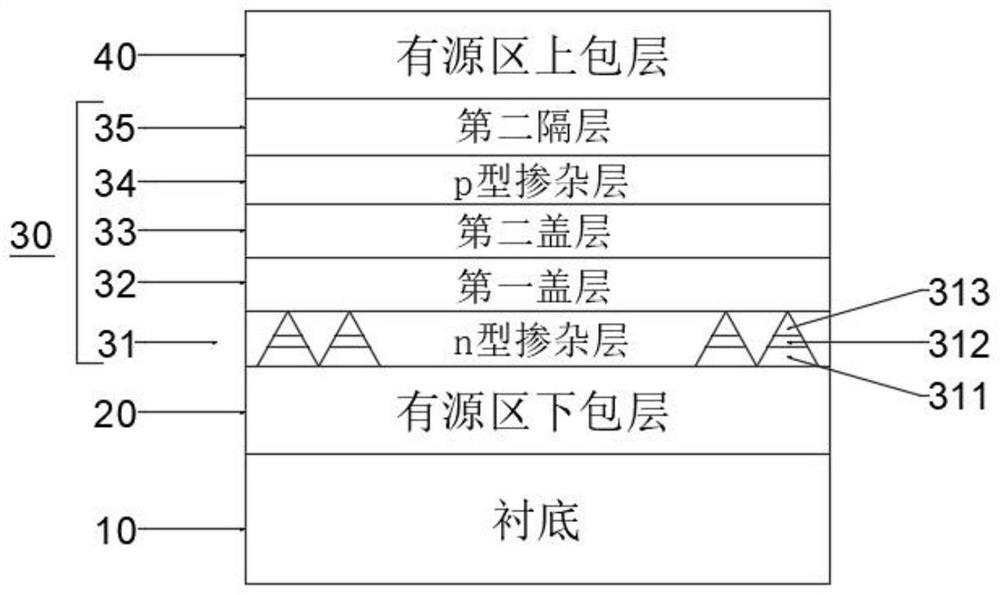
[0050] In order to make the object, technical solution and advantages of the present invention clearer, the present invention will be further described in detail below in conjunction with specific embodiments and with reference to the accompanying drawings.

[0051] figure 1 It is a schematic diagram of the double-doped quantum dot active region epitaxial structure.

[0052] Such as figure 1 As shown, the double-doped quantum dot active region epitaxial structure, the quantum dot active region 30 is configured as a periodic double-doped quantum dot stack structure, the quantum dot active region 30 includes: periodically arranged n-type doped impurity layer 31 and p-type doped layer 34 .

[0053] According to an embodiment of the present invention, the p-type doped layer 34 cooperates with the n-type doped layer 31 .

[0054] By forming a space-separated N-P-N~P-N-P alternately doped structure in the quantum dot active region 30, the non-radiative recombination center around...


PUM

PropertyMeasurementUnit
thicknessaaaaaaaaaa
thicknessaaaaaaaaaa
thicknessaaaaaaaaaa

Abstract

The invention discloses a double-doped quantum dot active region epitaxial structure and a preparation method and application thereof, a quantum dot active region of the double-doped quantum dot active region epitaxial structure is configured as a periodic double-doped quantum dot laminated structure, and the quantum dot active region comprises an n-type doped layer and a p-type doped layer which are periodically arranged; wherein the p-type doped layer and the n-type doped layer generate a synergistic effect, and the first interlayer is arranged between the n-type doped layer and the p-type doped layer which are periodically arranged; the second interlayer is arranged on the other side of the p-type doped layer, and the other side of the second interlayer is different from the side where the first interlayer is located; the first interlayer or the second interlayer is used for providing stress regulation or stress relief, and through a spatially separated alternate doping structure, the loss of current carriers is reduced, and the optical quality of the material is improved; the asymmetry of quasi-Fermi level movement of conduction bands and valence bands of the quantum dots is improved, and the peak gain and differential gain of the material are improved.

Description

technical field [0001] The invention relates to the technology in the field of semiconductor technology, in particular to a dual-doped quantum dot active region epitaxial structure and a preparation method and application thereof. Background technique [0002] The optical communication system is an important infrastructure of the modern information society. With the continuous development of new services such as cloud computing, Internet of Everything, and virtual reality, the traffic of the optical communication system is increasing exponentially, and its power consumption is also increasing explosively. The semiconductor laser is the core component of the optical fiber communication system. The huge amount of data and power consumption put forward the demand for high speed, low power consumption and low cost. Because the size of quantum dot materials in three dimensions is close to the de Broglie wavelength of electrons, it has discrete energy levels similar to atoms, and ...

Claims


Application Information

Patent Timeline
Patent Type & Authority Applications(China)
IPC IPC(8): H01S5/30H01S5/34H01S5/343H01L31/0304H01L31/0352
CPCH01S5/3086H01S5/3403H01S5/343H01S5/34313H01S5/3412H01L31/03042H01L31/035218
Inventor 汪帅杨涛吕尊仁
Owner INST OF SEMICONDUCTORS - CHINESE ACAD OF SCI
Why Eureka
Try Eureka