Preparation method of carbon-doped insulating layer, HEMT device and preparation method of HEMT device

An insulating layer and device technology, which is applied in semiconductor/solid-state device manufacturing, semiconductor devices, electrical components, etc., can solve the problem of large leakage current of carbon-doped insulating layer, large lattice mismatch of non-epitaxial layer, poor heat dissipation performance of devices, etc. problem, achieve good current density, good thermal conductivity, and improve performance

Active Publication Date: 2022-05-13
深圳市红与蓝企业管理中心(有限合伙)
View PDF5 Cites 0 Cited by
  • Summary
  • Abstract
  • Description
  • Claims
  • Application Information

AI Technical Summary

Problems solved by technology

[0007] The purpose of the present invention is to provide a HEMT device to solve the technical problems of existing HEMT devices such as poor heat dissipation performance, high price, inability to work under relatively high temperature conditions, large lattice mismatch of the epitaxial layer, and large defect density
[0008] Another object of the present invention is to provide a method for preparing a carbon-doped insulating layer which solves the technical problem of large leakage current of the existing carbon-doped insulating layer
[0009] Another object of the present invention is to provide a method for preparing a HEMT device, so as to solve the technical problems that the existing HEMT device preparation method is complicated, and the prepared device has poor heat dissipation performance and poor interface performance.

Method used

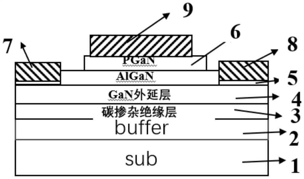
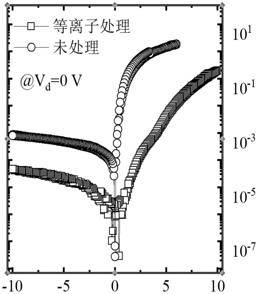

Image

  • Preparation method of carbon-doped insulating layer, HEMT device and preparation method of HEMT device
  • Preparation method of carbon-doped insulating layer, HEMT device and preparation method of HEMT device

Examples


Embodiment Construction

[0045] In order to make the technical problems, technical solutions and beneficial effects to be solved by the present invention clearer, the present invention will be further described in detail below in conjunction with the embodiments. It should be understood that the specific embodiments described here are only used to explain the present invention, not to limit the present invention.

[0046] In the embodiments of the present invention, the following nouns are described as follows.

[0047] HEMT device: High Electron Mobility Transistor, high electron mobility transistor.

[0048] MOCVD method: MOCVD uses organic compounds of group III and group II elements and hydrides of group V and group VI elements as crystal growth source materials, and performs vapor phase epitaxy on the substrate by thermal decomposition reaction to grow various III-V Thin-layer single-crystal materials of main group, II-VI subgroup compound semiconductors and their multiple solid solutions.

[0...


PUM

PropertyMeasurementUnit
thicknessaaaaaaaaaa
thicknessaaaaaaaaaa
thicknessaaaaaaaaaa

Abstract

The invention aims to provide a preparation method of a carbon-doped insulating layer, an HEMT device and a preparation method of the HEMT device, and compared with the prior art, the preparation method of the carbon-doped insulating layer is simple, efficient and practical. Plasma enhanced carbon ion implantation increases the activity and uniformity of C. As C enters the energy level of gallium nitride, a high-resistance region is formed, electric leakage of the device can be effectively blocked, the leakage current of the prepared carbon-doped insulating layer is greatly reduced, and the performance of the device is greatly improved. The HEMT device has the advantages of high resistivity, high electron mobility and low leakage current. Compared with a traditional device, the device has the advantages of good current density, low leakage current, higher device breakdown voltage and good thermal conductivity, so that the device can work under a relatively high temperature condition. And through the self-supporting substrate material, the problems of large lattice mismatch and large defect density of the existing epitaxial layer are solved, the interface performance is improved, and the performance and the yield of the HEMT device are further improved.

Description

technical field [0001] The invention belongs to the field of device manufacturing in semiconductor technology, and in particular relates to a HEMT device and a preparation method thereof. Background technique [0002] GaN-based materials have a series of material performance advantages such as large bandgap width, high breakdown field strength, high polarization coefficient, high electron mobility and electron saturation drift speed, and are the preferred materials for the preparation of a new generation of high-performance power electronic devices. application prospects. GaN-based materials are very attractive for both optoelectronic and microelectronic devices. GaN-based materials have the characteristics of forbidden bandwidth, high breakdown voltage, high electron saturation drift velocity, and good thermal stability, and can form an ideal heterojunction with AlGaN alloy materials, and the large conduction band shift on the heterointerface and the The high piezoelectri...

Claims


Application Information

Patent Timeline
Patent Type & Authority Applications(China)
IPC IPC(8): H01L29/06H01L29/778H01L21/02H01L21/3115H01L21/335
CPCH01L29/7787H01L29/66462H01L29/0638H01L21/0234H01L21/02321H01L21/3115Y02P70/50
Inventor 刘新科林峰李博黄双武宋利军黎晓华
Owner 深圳市红与蓝企业管理中心(有限合伙)
Why Eureka
Try Eureka