Silicon carbide separation gate MOSFET cell of integrated gate-controlled diode and preparation method thereof

A technology of gate-controlled diodes and silicon carbide, which is applied in the manufacture of diodes, electrical components, semiconductors/solid-state devices, etc., can solve the problems of high conduction voltage drop of SiC body diodes, increased dynamic losses of devices, and high density of JFET regions, etc., to achieve Effects of improving long-term reliability, reducing Miller capacitance, and reducing conduction voltage

Active Publication Date: 2022-05-27
NOVUS SEMICON CO LTD
View PDF16 Cites 1 Cited by
  • Summary
  • Abstract
  • Description
  • Claims
  • Application Information

AI Technical Summary

Problems solved by technology

[0004] However, there are two problems in the planar SiC VDMOS. One is that the density of the JFET area is relatively high, which introduces a large Miller capacitance, which increases the dynamic loss of the device; the other is that the parasitic SiC body diode conduction voltage drop is too high. , and it is a bipolar device, which has a large reverse recovery current. In addition, the bipolar degradation phenomenon caused by the silicon carbide BPD defect makes the conduction voltage drop of the body diode continue to increase with the growth of service time. Therefore, The body diode of SiC VDMOS cannot be directly used as a freewheeling diode

Method used


Image

  • Silicon carbide separation gate MOSFET cell of integrated gate-controlled diode and preparation method thereof
  • Silicon carbide separation gate MOSFET cell of integrated gate-controlled diode and preparation method thereof
  • Silicon carbide separation gate MOSFET cell of integrated gate-controlled diode and preparation method thereof

Examples


Embodiment Construction

[0045] The principles and features of the present invention will be described below with reference to the accompanying drawings. The examples are only used to explain the present invention, but not to limit the scope of the present invention.

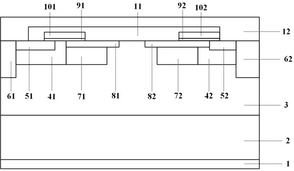
[0046] This embodiment provides a silicon carbide split gate MOSFET cell with integrated gated diode, such as figure 1 As shown, it includes a backside ohmic contact alloy 1, an N-type doped silicon carbide substrate 2, an N-type doped silicon carbide epitaxial layer 3, a first P-type doped well region 41, a second P-type doped well region 42, The first N-type doped source region 51, the second N-type doped source region 52, the first P-type doped source region 61, the second P-type doped source region 62, the first P-type doped buried layer 71, The second P-type doped buried layer 72, the first N-type doped guide layer 81, the second N-type doped guide layer 82, the first gate oxide layer 91, the second gate oxide layer 92, the first p...


PUM


Abstract

The invention relates to a silicon carbide separation gate MOSFET (Metal-Oxide-Semiconductor Field Effect Transistor) cell integrated with a gate-controlled diode and a preparation method thereof, belonging to the technical field of power semiconductor devices. The MOSFET adopts a separation gate design to reduce the switching loss of the device; in order to solve the problem that the reliability of gate oxide is reduced due to a separation gate structure, a P-type buried layer is added to reduce the electric field intensity of a gate oxide layer at the edge of polycrystalline silicon; an N-type diversion layer is added, and current is introduced into a drift region of the device from a channel; in order to reduce the conduction voltage drop of a parasitic body diode of the silicon carbide MOSFET so as to reduce the reverse recovery current of the body diode, a grid control diode based on an accumulation type channel MOS structure is introduced to the other side of a cell of the MOSFET. According to the invention, the accumulation type channel is adopted to fully reduce the conduction loss of the diode, and the source electrode metal is in contact with the polycrystalline silicon of the grid control diode on the side wall by etching and filling the metal, so that the cell size is reduced.

Description

technical field [0001] The invention belongs to the technical field of power semiconductor devices, and in particular relates to a silicon carbide separated gate MOSFET cell with integrated gate-controlled diode and a preparation method thereof. Background technique [0002] The wide-bandgap semiconductor material SiC is an ideal material for the preparation of high-voltage power electronic devices. Compared with Si material, SiC material has a high breakdown electric field strength (4×10 6 V / cm), high carrier saturation drift velocity (2×10 7 cm / s), high thermal conductivity, good thermal stability, etc., so it is especially suitable for high-power, high-voltage, high-temperature and radiation-resistant electronic devices. [0003] SiC VDMOS is a commonly used device in SiC power devices. Compared with bipolar devices, since SiCVDMOS has no charge storage effect, it has better frequency characteristics and lower switching losses. At the same time, the wide band gap of SiC...

Claims


Application Information

Patent Timeline
Patent Type & Authority Applications(China)
IPC IPC(8): H01L29/423H01L29/06H01L29/10H01L29/417H01L29/45H01L29/78H01L21/336H01L21/28
CPCH01L29/7804H01L29/66068H01L29/0696H01L29/42356H01L29/1037H01L29/41741H01L29/45H01L29/401Y02B70/10
Inventor 顾航高巍戴茂州
Owner NOVUS SEMICON CO LTD
Why Eureka
Try Eureka