A coaxial bicyclic TSV structure with low thermal stress and high electrical performance and preparation method thereof
A high electrical performance, coaxial technology, applied in the direction of circuits, electrical components, electrical solid devices, etc., can solve the problems of increasing static power consumption, signal distortion, leakage current, etc., achieve convenient and easy process, reduce thermal stress, Effect of reducing static loss
- Summary
- Abstract
- Description
- Claims
- Application Information
AI Technical Summary
Problems solved by technology
Method used
Image
Examples
Embodiment 1
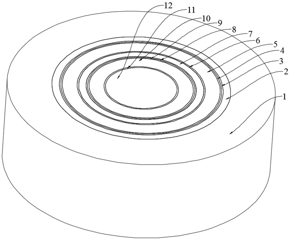
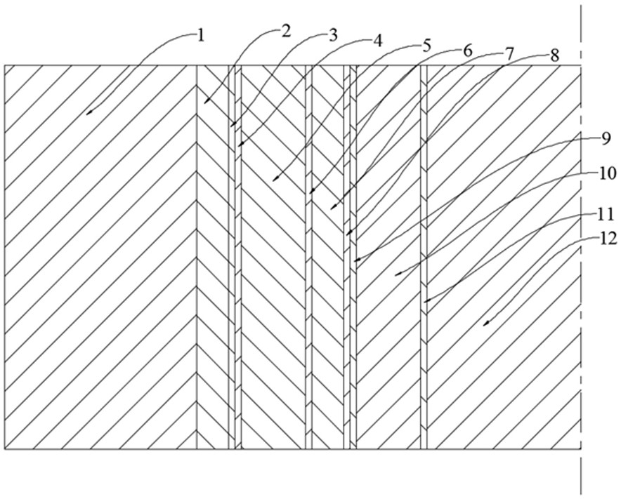
[0040] like figure 1 and figure 2 As shown, the present invention provides a coaxial double-ring TSV structure with low thermal stress and high electrical performance, including a first insulating layer 2, a first diffusion adhesion layer / barrier that are coaxially processed on a wafer 1 sequentially from outside to inside Layer 3, first seed layer 4, outer conductive metal ring 5, second diffusion adhesion layer / barrier layer 6, second insulating layer 7, third diffusion adhesion layer / barrier layer 8, second seed layer 9, inner A conductive metal ring 10, a fourth diffusion adhesion layer / barrier layer 11 and a third insulating layer 12 as a filling core.
[0041] The insulating materials of the first insulating layer 2 , the second insulating layer 7 and the third insulating layer 12 are inorganic insulating materials or organic insulating materials. The inorganic insulating materials include oxides, nitrides, carbides and oxynitrides (insulating ceramic materials), and ...
Embodiment 2
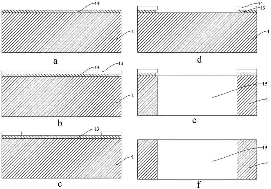
[0043] Example 2: as image 3 and Figure 4 As shown, the present invention also provides a method for preparing a coaxial bicyclic TSV structure with low thermal stress and high electrical performance, comprising the following steps:
[0044] Step 1, pre-processing the wafer 1, and finely grinding the front side of the wafer 1 to the required thickness;
[0045] After grinding, the thickness of the wafer 1 is 5-40 μm, in this embodiment, it is 30 μm;
[0046] Step 2, forming TSV through holes 15 on the front side of the preprocessed wafer 1;
[0047] like image 3 As shown, the method of making the TSV via 15 is as follows:
[0048] Step 2.1, such as image 3As shown in (a), a thin film 13 is deposited on the front surface of the wafer 1; the deposited thin film 13 can be an oxide, a nitride, carbide, oxynitride and other insulating films, or an inorganic material, Organic polymer materials, semiconductor materials, metal materials, ceramic materials and other thin film...
PUM
| Property | Measurement | Unit |
|---|---|---|
| thickness | aaaaa | aaaaa |
| surface roughness | aaaaa | aaaaa |
| thickness | aaaaa | aaaaa |
Abstract
Description
Claims
Application Information


