Wavelength division multiplexing system with power balancing effect and preparation method thereof

A technology of wavelength division multiplexing and wavelength division multiplexer, which is applied to optical waveguides, optical waveguides, coupling of optical waveguides, instruments, etc., which can solve the problem of low signal strength and receiver sensitivity, the receiver cannot detect the signal, and the received energy is unbalanced. and other problems, to achieve the effect of improving system stability, compact structure and reducing preparation cost

Active Publication Date: 2022-06-03
JILIN UNIV
View PDF7 Cites 0 Cited by
  • Summary
  • Abstract
  • Description
  • Claims
  • Application Information

AI Technical Summary

Problems solved by technology

[0004] 1. The unbalanced receiving energy will eventually lead to energy fluctuations exceeding the dynamic range allowed by the receiver;
[0005] 2. The imbalance of the cumulative signal-to-noise ratio (Signal Noise Rate, SNR) will lead to an increase in the bit error rate (Bite Error Rate, BER) for a certain wavelength;
[0006] 3. Due to insufficient gain, the signal strength of the smallest channel may be lower than the sensitivity of the receiver, resulting in the receiver being unable to detect the signal
As the number of channels in the WDM system increases, the number of connected VOAs will also increase, and the wavelengths covered will become more, and the power imbalance in the channels will also increase accordingly. In order to reduce design and manufacturing costs, it has power balance Functional WDM system urgently needs to be developed

Method used


Image

  • Wavelength division multiplexing system with power balancing effect and preparation method thereof
  • Wavelength division multiplexing system with power balancing effect and preparation method thereof
  • Wavelength division multiplexing system with power balancing effect and preparation method thereof

Examples


Embodiment 1

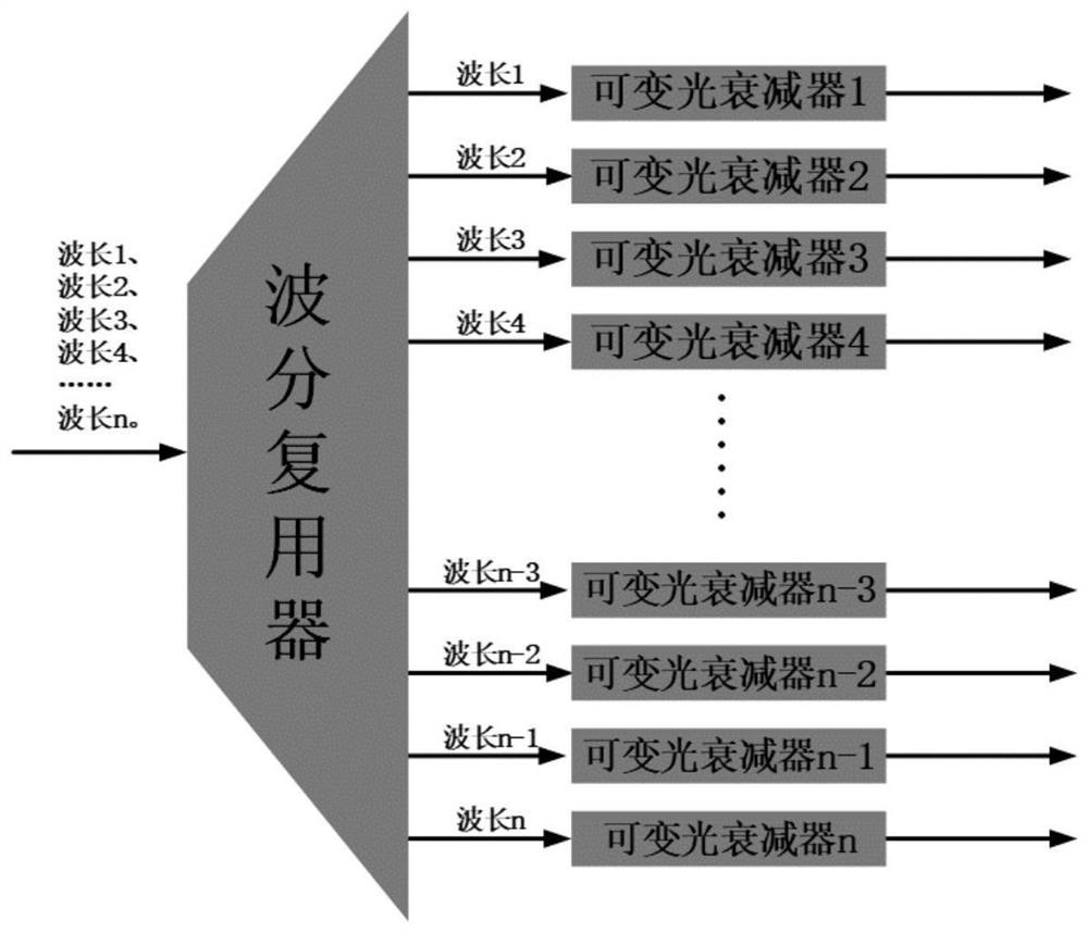
[0041] as attached figure 1 As shown, the wavelength division multiplexer and the variable optical attenuator array are integrated on the same chip, and multiple wavelengths are input into the wavelength division multiplexer. The light is divided into different channels and then into different variable optical attenuators. Due to the power imbalance between channels, the power balance of the output channels is achieved by tuning the variable optical attenuators.

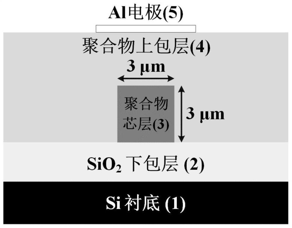
[0042] as attached figure 2 As shown, from bottom to top, the first modulation arm waveguide (300) is composed of Si substrate (1), SiO 2 The lower cladding layer (2), the polymer core layer (3), the polymer upper cladding layer (4) and the metal electrode (5) are composed (the structures of the remaining waveguides are the same, except that there is no metal electrode (5) part). The SiO 2 The lower cladding layer (2) can be grown by thermal oxidation or PECVD (Plasma Enhanced Chemical Vapor Deposition) depositi...


PUM

PropertyMeasurementUnit
thicknessaaaaaaaaaa
thicknessaaaaaaaaaa
thicknessaaaaaaaaaa

Abstract

The invention discloses a wavelength division multiplexing system with a power balancing function and a preparation method thereof, and belongs to the technical field of silicon dioxide/polymer mixed waveguide optical integrated chips. The multi-channel wavelength division multiplexer and the variable optical attenuator array are integrated on the same chip, a wide-spectrum light source is coupled into the wavelength division multiplexer, and light with different wavelengths is divided into different channels through the wave division effect of the wavelength division multiplexer and then enters different variable optical attenuators; because the power among the channels of the wavelength division multiplexer is unbalanced, the power balance of the output channels can be realized by tuning the variable optical attenuator. According to the wavelength division multiplexing system with the power balancing function, the silicon dioxide/polymer mixed waveguide PLC technology is adopted, and the power consumption of the system is reduced by utilizing the advantages that the silicon dioxide lower cladding is good in heat dissipation and low in loss and the thermo-optical coefficient of the polymer core layer and the polymer upper cladding is large. The method is very suitable for the fields of optical communication, optical calculation and the like, and has a very strong application prospect.

Description

technical field [0001] The invention belongs to the technical field of silicon dioxide / polymer hybrid waveguide optical integrated chips, in particular to a wavelength division multiplexing system with power equalization and a preparation method thereof. Background technique [0002] Planar Lightwave Circuit (PLC) because its process is compatible with Complementary Metal Oxide Semiconductor (CMOS) process, it is easy to realize miniaturized and integrated multi-functional photonic integrated chips, and has won scientific research units, Extensive research in colleges and universities, and occupy a certain market. Polymer PLC devices prepared with polymer materials have the advantages of simple preparation process, low cost, low loss, and high coupling efficiency with optical fibers. In particular, the thermo-optic coefficient of polymer materials is an order of magnitude higher than that of silica, which is very suitable for The preparation of low-power thermo-optic device...

Claims


Application Information

Patent Timeline
Patent Type & Authority Applications(China)
IPC IPC(8): G02B6/12G02B6/293G02B6/26
CPCG02B6/12007G02B6/2938G02B6/29301G02B6/266G02B2006/12164
Inventor 尹悦鑫姚梦可李悦丁颖智曹至庚许馨如张大明
Owner JILIN UNIV
Why Eureka
Try Eureka