Ultraviolet LED epitaxial structure and growth method thereof
A technology of epitaxial structure and growth method, which is applied in the direction of electrical components, circuits, semiconductor devices, etc., can solve the problems of restricted application and low luminous efficiency, and achieve the effect of improving crystal quality, high luminous efficiency and good crystal quality
- Summary
- Abstract
- Description
- Claims
- Application Information
AI Technical Summary
Problems solved by technology
Method used
Image
Examples
Embodiment 1
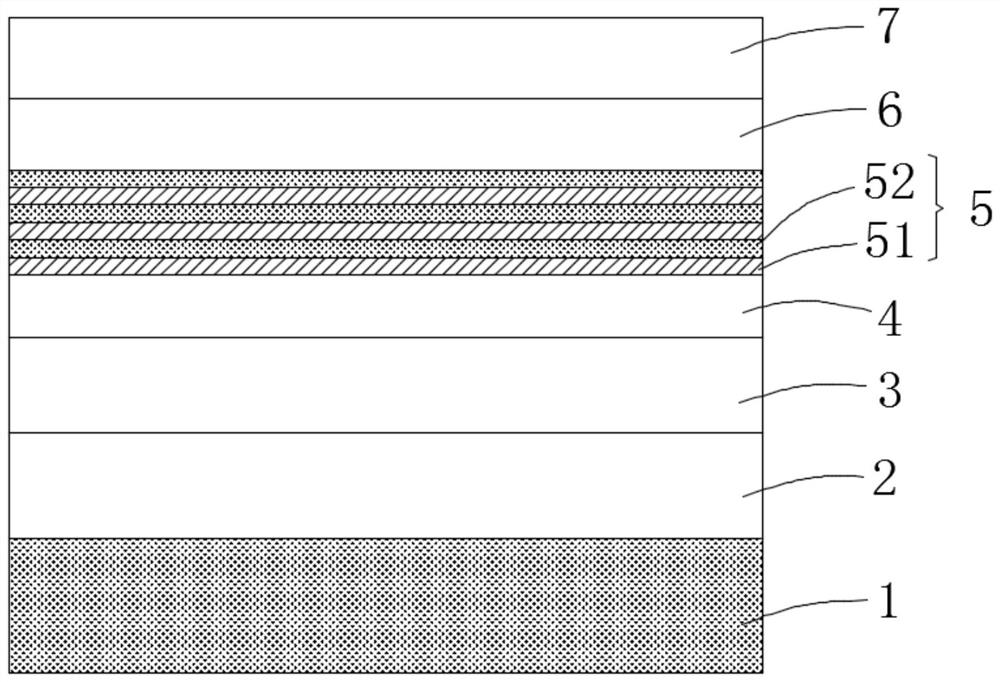
[0034] An ultraviolet LED epitaxial structure, such as figure 1 As shown, it includes: sequentially growing a buffer layer 2 , an unintentional doped layer 3 , an n-type doped layer 4 , a multiple quantum well light-emitting layer 5 , an EBL layer 6 and a p-type AlGaN layer 7 on the substrate 1 .
[0035] The substrate 1 is sapphire; the buffer layer 2 includes an AlN layer, an AlGaN layer and an AlInGaN layer grown in sequence; the unintentional doped layer 3 is AlN; the n-type doped layer 4 is n-AlN; The multiple quantum well light-emitting layer 5 is (Al x Ga 1-x N / Al y Ga 1-y N) n , where x is 0.2, y is 0.3, and n is 5; the EBL layer 6 is a p-AlGaN barrier layer.
[0036] A method for growing an ultraviolet LED epitaxial structure, comprising the following steps:
[0037] 1. Growth buffer layer 2:
[0038] 1) An AlN layer is grown on the substrate 1. The growth temperature of the AlN layer is 700°C, the pressure is 50torr, the flow rate of TMAl is 50sccm, and the NH...
Embodiment 2
[0053] An ultraviolet LED epitaxial structure, such as figure 1 As shown, it includes: sequentially growing a buffer layer 2 , an unintentional doped layer 3 , an n-type doped layer 4 , a multiple quantum well light-emitting layer 5 , an EBL layer 6 and a p-type AlGaN layer 7 on the substrate 1 .
[0054] The substrate 1 is a silicon substrate 1; the buffer layer 2 includes an AlN layer, an AlGaN layer and an AlInGaN layer grown in sequence; the unintentional doped layer 3 is AlGaN; the n-type doped layer 4 is n -AlGaN; the multiple quantum well light-emitting layer 5 is (Al x Ga 1-x N / Al y Ga 1-y N) n , where x is 0.3, y is 0.5, and n is 7; the EBL layer 6 is a p-AlInGaN barrier layer.
[0055] A method for growing an ultraviolet LED epitaxial structure, comprising the following steps:
[0056] 1. Growth buffer layer 2:
[0057] 1) An AlN layer is grown on the substrate 1. The growth temperature of the AlN layer is 750°C, the pressure is 80torr, the flow rate of TMAl i...
Embodiment 3
[0072] An ultraviolet LED epitaxial structure, such as figure 1 As shown, it includes: sequentially growing a buffer layer 2 , an unintentional doped layer 3 , an n-type doped layer 4 , a multiple quantum well light-emitting layer 5 , an EBL layer 6 and a p-type AlGaN layer 7 on the substrate 1 .
[0073] The substrate 1 is silicon carbide; the buffer layer 2 includes an AlN layer, an AlGaN layer and an AlInGaN layer grown in sequence; the unintentional doped layer 3 is InAlGaN; the n-type doped layer 4 is n-InAlGaN ; The multiple quantum well light-emitting layer 5 is (Al x Ga 1-x N / Al y Ga 1-y N) n , where x is 0.4, y is 0.6, and n is 10; the EBL layer 6 is a p-AlN barrier layer.
[0074] A method for growing an ultraviolet LED epitaxial structure, comprising the following steps:
[0075] 1. Growth buffer layer 2:
[0076] 1) An AlN layer is grown on the substrate 1. The growth temperature of the AlN layer is 800°C, the pressure is 100torr, the flow rate of TMAl is 15...
PUM
| Property | Measurement | Unit |
|---|---|---|
| temperature | aaaaa | aaaaa |
| thickness | aaaaa | aaaaa |
| thickness | aaaaa | aaaaa |
Abstract
Description
Claims
Application Information
