Low-resistance high-reflection ohmic contact electrode and preparation method thereof
A technology of ohmic contact electrodes and high reflection, which is applied in the manufacture of circuits, electrical components, and final products. It can solve the problems of less research on p-type ohmic contacts and achieve high light transmittance, low resistivity, and high conductivity.
- Summary
- Abstract
- Description
- Claims
- Application Information
AI Technical Summary
Problems solved by technology
Method used
Image


Examples
Embodiment 1
[0048] like figure 1As shown, this embodiment discloses a method for preparing a low-resistance and high-reflection ohmic contact electrode. The ohmic contact electrode is prepared on a p-type semiconductor wafer, and the p-type semiconductor wafer is a p-type group III nitride. The p-type III-nitride is AlGaN, specifically, the p-type III-nitride is p-Al 0.4 Ga 0.6 N, its preparation method comprises the following steps:
[0049] S1: cleaning the surface of the p-type semiconductor wafer; the specific steps are:
[0050] S11: Use electronic grade acetone and isoacetone to clean the surface of the p-type semiconductor wafer in turn, and then clean with deionized water;
[0051] S12: use pure hydrochloric acid or hydrofluoric acid to soak the p-type semiconductor wafer, and the soaking time is 20-90s;
[0052] S13: Then use deionized water to clean the p-type semiconductor wafer;
[0053] S14: Dry the p-type semiconductor wafer with high-purity ammonia gas;
[0054] S2: u...
Embodiment 2
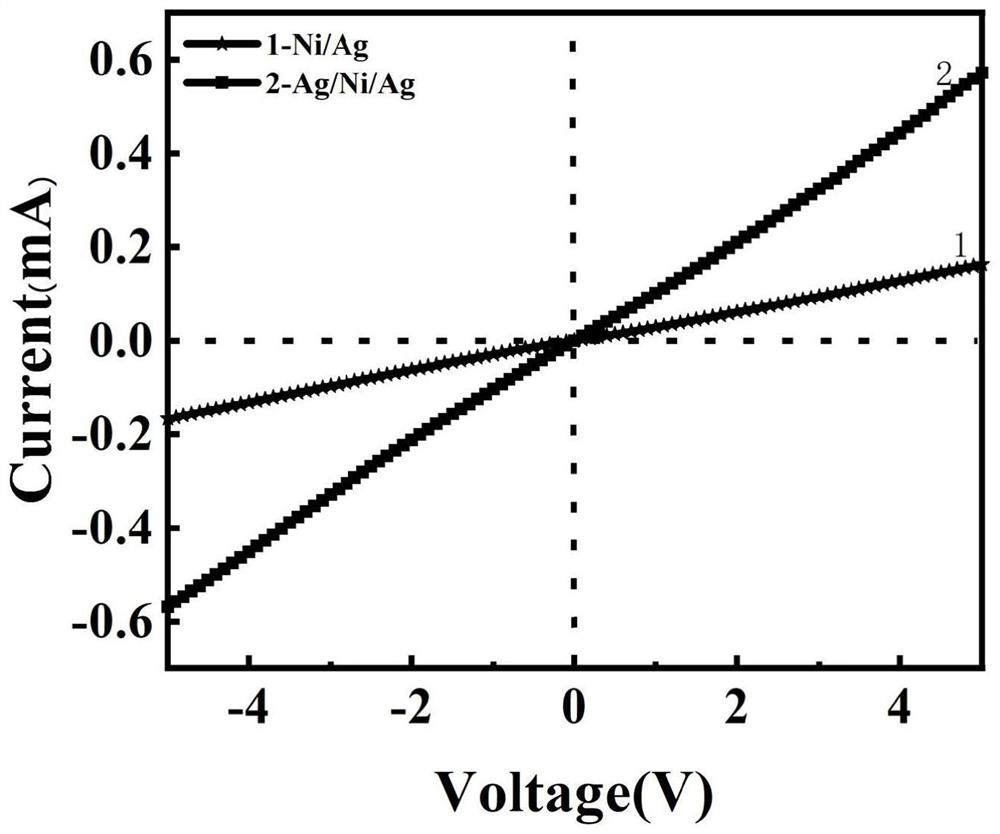
[0064] In this example, the electrical characteristic test of the ohmic contact electrode obtained in Example 1 was carried out.
[0065] The line segment 1 is a comparative example. The main difference between the comparative example and this embodiment is that in step S3 of the comparative example, only one layer of metallic silver and one layer of metallic nickel are deposited, namely Ni / Ag and p-Al 0.4 Ga 0.6 Ohmic contact electrodes formed by N;
[0066] Line segment 2 is the ohmic contact electrode obtained in Example 1, namely Ag / Ni / Ag and p-Al 0.4 Ga 0.6 Ohmic contact electrodes formed by N.
[0067] Test results such as figure 2 shown, from figure 2 It can be seen that both line segment 1 and line segment 2 exhibit linear behavior, indicating that both can interact with p-Al 0.4 Ga 0.6 N forms a good ohmic contact, but the slope of line segment 2 is larger, indicating that Ag / Ni / Ag and p-Al 0.4 Ga 0.6 The ohmic contact electrode formed by N has lower resist...
Embodiment 3
[0069] In this example, the optical characteristic test of the ohmic contact electrode obtained in Example 1 was carried out.
[0070] Wherein, line segment 1 is the ultraviolet light reflectance curve spectrum of the ohmic contact electrode obtained in Example 1 after annealing at 350°C;
[0071] Line segment 2 is the ultraviolet light reflectance curve spectrum of the ohmic contact electrode obtained in Example 1 after annealing at 450°C.
[0072] image 3 Optical properties of Ag / Ni / Ag / Al of the ohmic contact electrode obtained in Example 1 on a sapphire substrate. from image 3 It can be seen that the overall reflectivity of annealing at 350°C (line segment 1) is significantly higher than that of annealing at 450°C (line segment 2), indicating that the ohmic contact electrode of this embodiment is more favorable for obtaining high reflectivity at low temperatures, that is, 350 The samples annealed at ℃ (line 1) have higher light reflectance.
[0073] from image 3 It ...
PUM
| Property | Measurement | Unit |
|---|---|---|
| Thickness | aaaaa | aaaaa |
| Thickness | aaaaa | aaaaa |
| Thickness | aaaaa | aaaaa |
Abstract
Description
Claims
Application Information
 - R&D
- Intellectual Property
- Life Sciences
- Materials
- Tech Scout
- Unparalleled Data Quality
- Higher Quality Content
- 60% Fewer Hallucinations
Browse by: Latest US Patents, China's latest patents, Technical Efficacy Thesaurus, Application Domain, Technology Topic, Popular Technical Reports.
© 2025 PatSnap. All rights reserved.Legal|Privacy policy|Modern Slavery Act Transparency Statement|Sitemap|About US| Contact US: help@patsnap.com