

Thin film transistor and its producing method
A technology of thin film transistors and manufacturing methods, applied in the field of active matrix organic electroluminescent display devices
- Summary
- Abstract
- Description
- Claims
- Application Information
AI Technical Summary
Problems solved by technology
Method used
Image

Examples
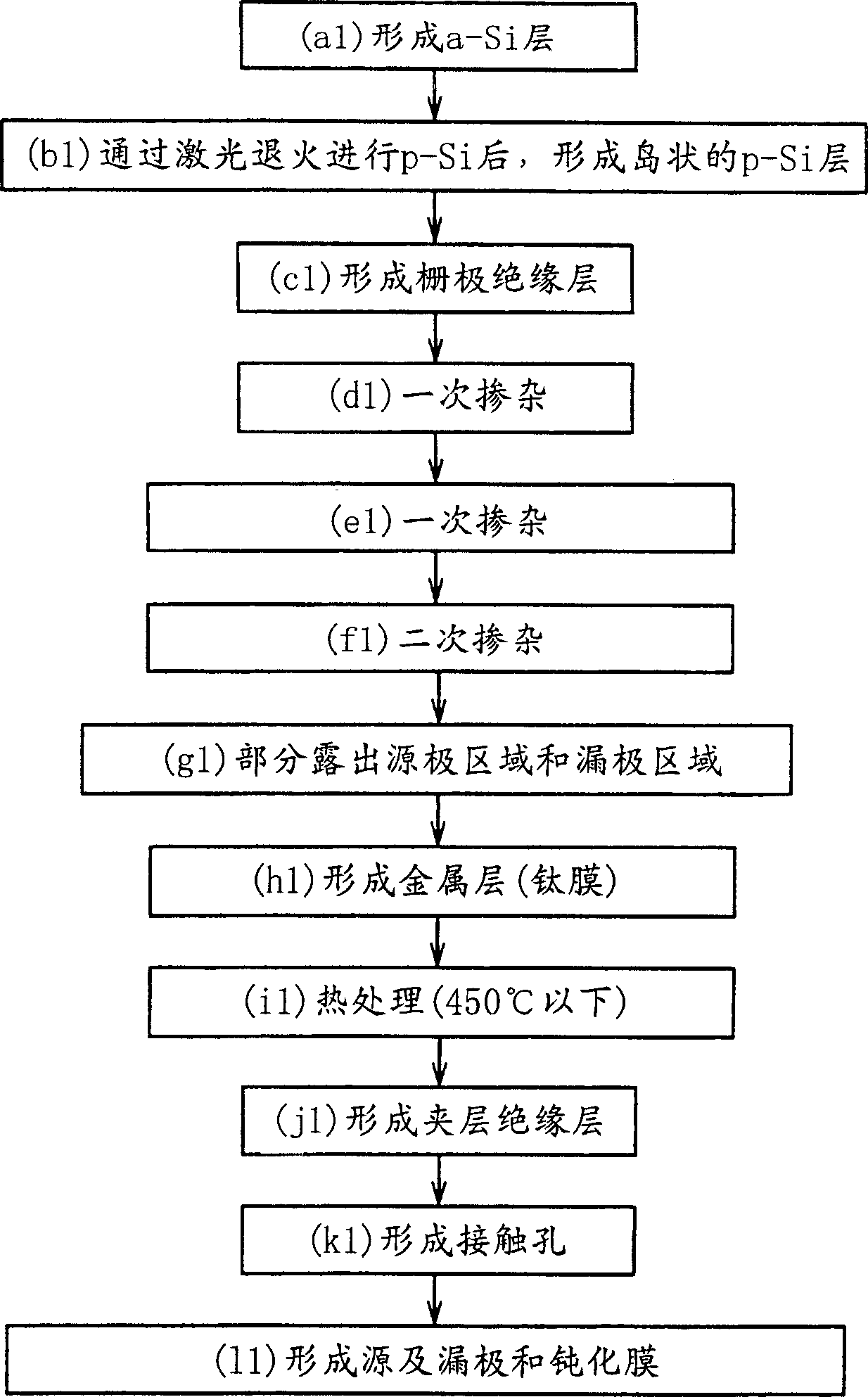
Embodiment 1
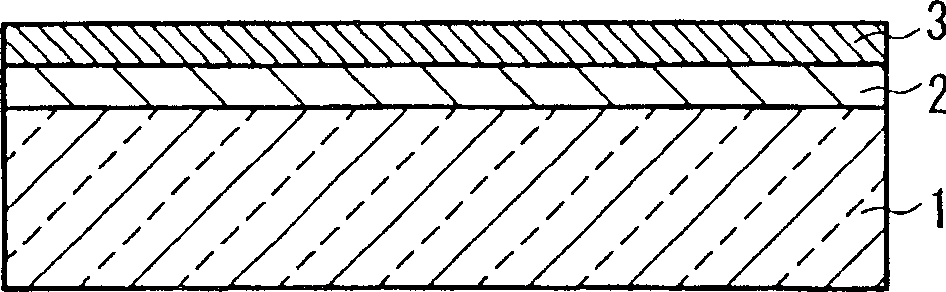
[0076] (a1) First, by plasma CVD or decompression CVD, the SiO on the glass substrate 1 2 An amorphous silicon layer (a-Si layer) 3 with a thickness of 50 nm is formed on the layer (undercoat layer) 2, and dehydrogenation treatment is performed at a temperature of 450° C. under a nitrogen atmosphere ( Figure 2A ).
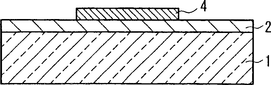
[0077] (b1) Next, by laser annealing using an excimer laser using XeCl, KrF, etc. as an excitation gas, molten crystallization (polysilicon) of the a-Si layer 3 is performed, and photolithography and etching are performed to form islands at predetermined positions. Shaped polysilicon layer (p-Si layer) 4 ( Figure 2B ).
[0078] (c1) Next, form SiO with a thickness of 100nm 2 layer, as the gate insulating layer 5, covering the p-Si layer 4 ( Figure 2C ).
[0079] (d1) Afterwards, the MoW alloy is formed into a film with a thickness of about 400-500 nm by sputtering, etc., and the MoW alloy layer is formed by photolithography and corrosion, as the gate 6 ( ...
Embodiment 2
[0094] In this embodiment, first, the same as in embodiment 1, (a1)-(e1) (refer to figure 1 ,2).
[0095] (f2) Next, a photoresist mask 30 having openings on the surface of the region consisting of the source region and the drain region is formed, and secondary doping is performed. A photoresist 30 is formed to cover the gate 6 . For example, by taking a dose of 1 x 10 14 piece / cm 2 Phosphorus ions are implanted for doping. Thus, at the same time as the channel region 7 is formed, the LDD regions 9a, 9b, the source region 10, and the drain region 11 ( Figure 3A ).
[0096] (g2) Next, metal ions (titanium ions) are implanted without removing the resist mask 30 . When titanium ions are implanted in this way, titanium ions are implanted into the same region as that into which impurity ions are secondarily introduced (the region constituted by the source region and the drain region). Also can use other metal ions such as cobalt, nickel to replace titanium ion ( Figure 3...
Embodiment 3
[0102] (a3) First, the SiO on the glass substrate 1 2 On the layer (undercoat layer) 2, island-shaped metal layers (titanium films) 12a, 12b with a thickness of 20nm are formed by sputtering at positions corresponding to source and drain regions to be formed later. Here, other metal layers such as cobalt and nickel can also be used instead of the titanium film ( Figure 4A ).
[0103] (b3) Next, form an amorphous silicon layer (a-Si layer) 3 with a thickness of 50 nm on the metal layer (titanium film) 2 by plasma CVD or decompression CVD, and heat it at 450 degrees under a nitrogen atmosphere. temperature for dehydrogenation ( Figure 4B ).
[0104] (c3) Next, by laser annealing using an excimer laser using XeCl, KrF, etc. as an excitation gas, molten crystallization (polysilicon) of the a-Si layer 3 is performed, and photolithography and etching are performed to form an island-shaped polysilicon layer ( p-Si layer)4( Figure 4C ).
[0105] After (d3), SiO with a thickne...
PUM
| Property | Measurement | Unit |
|---|---|---|
| Thickness | aaaaa | aaaaa |
| Thickness | aaaaa | aaaaa |
| Thickness | aaaaa | aaaaa |
Abstract
Description
Claims
Application Information