

Mfg. method of electronic parts and siad electronic parts, electroless coating method
A technology of electronic components and manufacturing methods, applied to the manufacture of electronic components and the electronic components, can solve the problems of complex manufacturing process, increased production cost, thickened film thickness, etc., and achieve the effect of low cost and low reliability
- Summary
- Abstract
- Description
- Claims
- Application Information
AI Technical Summary
Problems solved by technology
Method used
Image

Examples
Embodiment 1
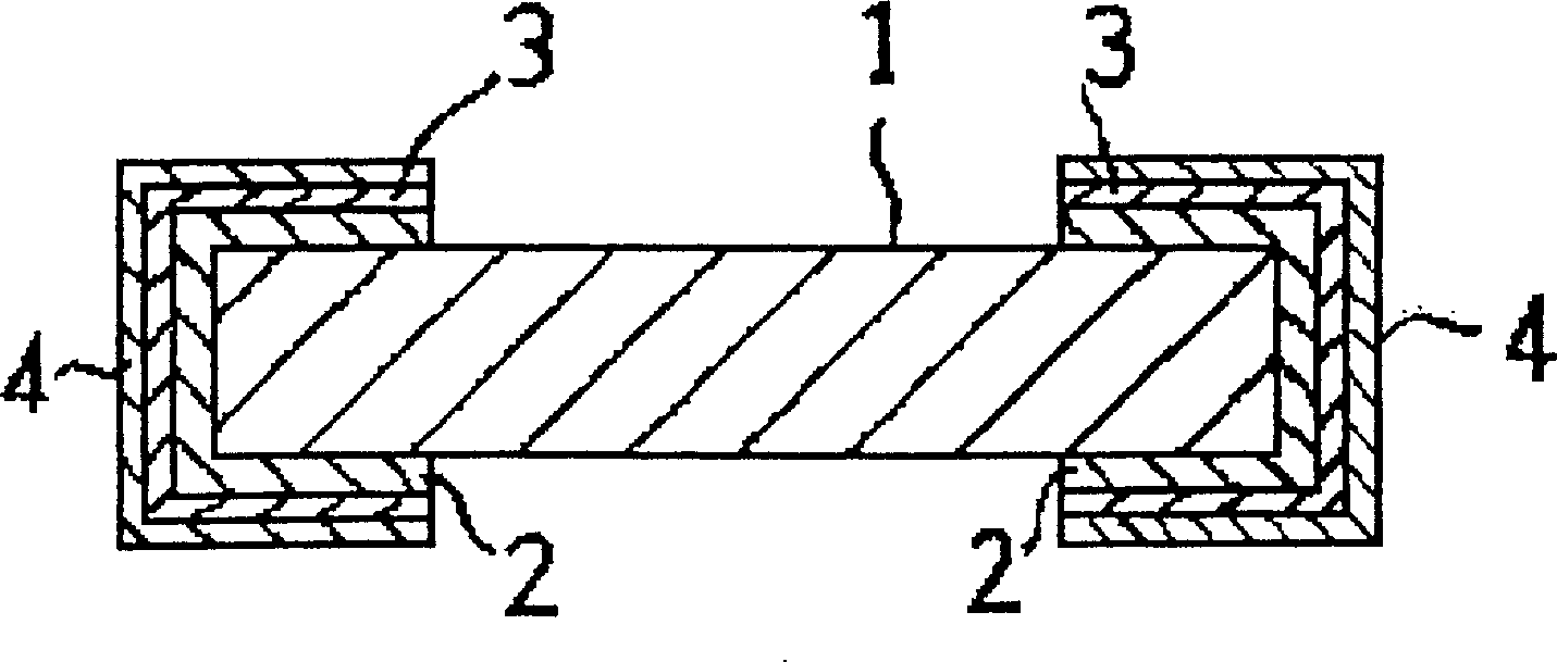
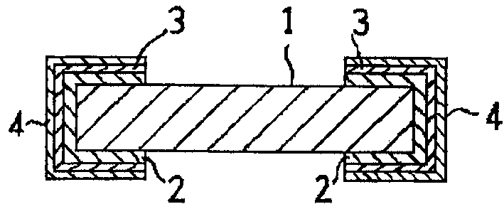
[0148] The present inventors formed Cu electrodes on both ends of a ceramic substrate having a length of 3.2 mm, a width of 1.6 mm, and a thickness of 1.0 mm, and produced 10 objects to be plated.
[0149] Then, the inner volume of the plating bath (the first plating bath) filled with the following composition is 1.90×10 -4 m 3 Dip the above 10 objects to be plated in the drum, and add 7.9g (about 1500 pieces) of Ni sheets with a diameter of about 1mm into the drum at the same time, for 0.05s -1 The drum was rotated at a rotation speed (=3 rpm) for 30 minutes to perform autocatalytic plating, and a Ni—P plated film was formed on the surface of the Cu electrode.
[0150] [Composition of the first plating bath]
[0151] Metal salt: nickel chloride 30.0kg / m 3
[0152] Reducing agent: sodium hypophosphite 10.0kg / m 3
[0153] Complexing agent: sodium citrate 10.0kg / m 3
[0154] Sodium glycolate 10.0kg / m 3
[0155] pH: 4.2
[0156] Bath temperature: 85°C
[0157]...
Embodiment 2
[0165] As in Example 1, Ag-Pd electrodes were formed on both ends of the ceramic substrate. Then, Ni-P coating film and Au coating film were formed on the surface of Ag-Pd electrode according to the same procedure as Example 1, and the test piece of Example 2 was obtained.
Embodiment 3
[0167] As in Example 1, Ag electrodes were formed on both ends of the ceramic substrate. Then, a Ni-P coating film and an Au coating film were formed on the surface of the Ag electrode according to the same procedure as in Example 1 to prepare the test piece of Example 3.
[0168] Table 2 shows the film thickness of each example.
[0169] For the film thickness, a fluorescent X-ray thickness gauge (SEA5120 manufactured by Seiko Instruments Co., Ltd.) was used.
[0170] electrode material
Film thickness (μm)
Ni-P coating
Au coating
Reality
apply
example
1
Cu
5.43
0.20
2
Ag-Pd
5.21
0.08
3
Ag
4.15
0.03
[0171] It can be confirmed from Table 2 that even sodium p-hypophosphite (NaH 2 PO 2) Electrode materials that do not show catalytic activity can also form Ni-P coatings on the electrode surface by self-catalytic plating...
PUM
| Property | Measurement | Unit |
|---|---|---|
| Film thickness | aaaaa | aaaaa |
| Diameter | aaaaa | aaaaa |
Abstract
Description
Claims
Application Information