Method for oriented growth of diamond film on aluminium oxide ceramic

A technology of alumina ceramics and diamond films, which is applied in the direction of gaseous chemical plating, metal material coating process, coating, etc., can solve problems such as the difficulty of directional growth, and achieve the effect of improving comprehensive performance

Inactive Publication Date: 2003-11-26
SHANGHAI UNIV
View PDF0 Cites 15 Cited by
  • Summary
  • Abstract
  • Description
  • Claims
  • Application Information

AI Technical Summary

Problems solved by technology

Therefore, it is much more difficult to realize the directional growth of diamond films on alumina ceramics than on silicon substrates. So far, there has been no report on directional growth of diamond films on ceramic substrates.

Method used


Image

  • Method for oriented growth of diamond film on aluminium oxide ceramic
  • Method for oriented growth of diamond film on aluminium oxide ceramic
  • Method for oriented growth of diamond film on aluminium oxide ceramic

Examples


Embodiment 1

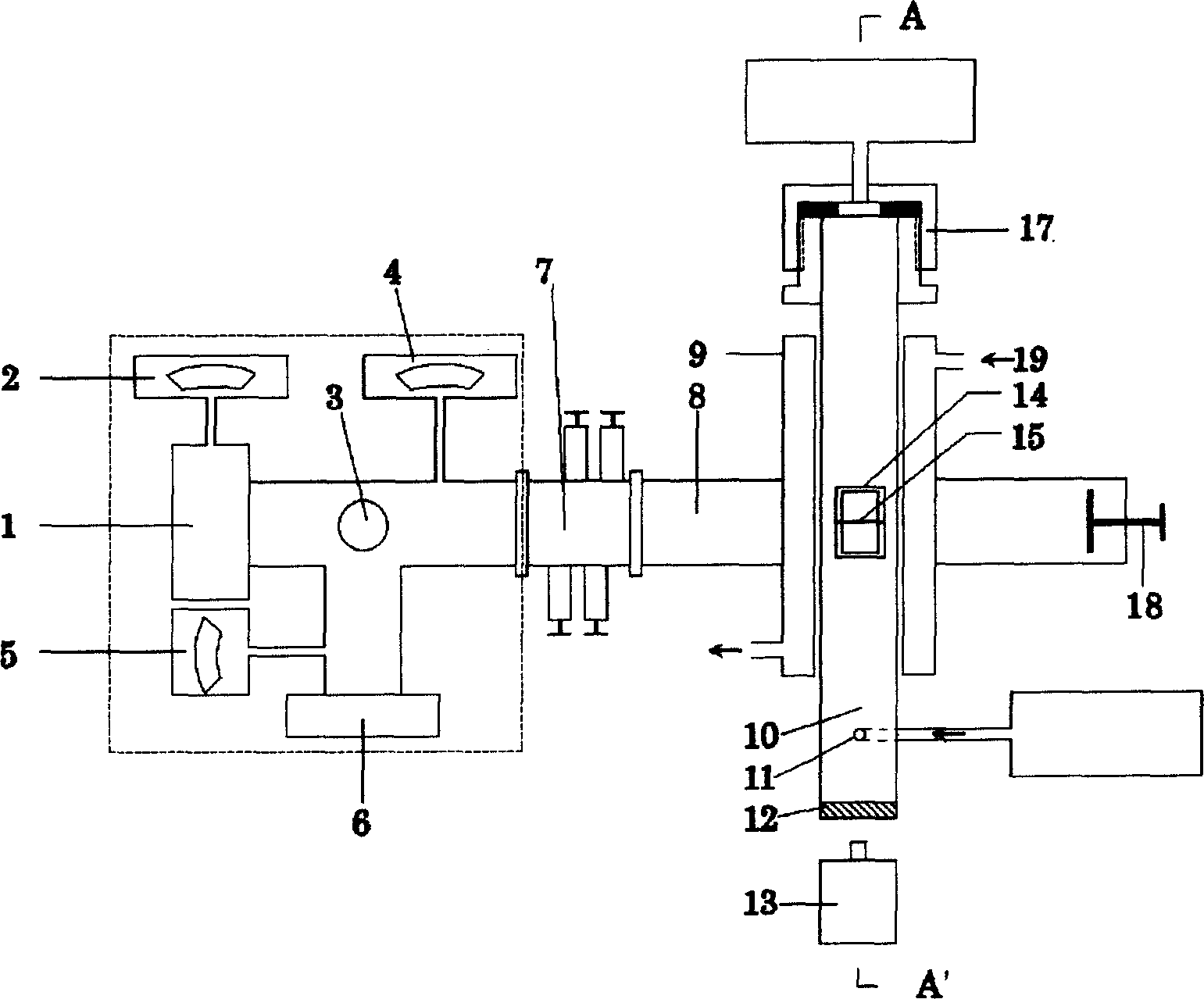
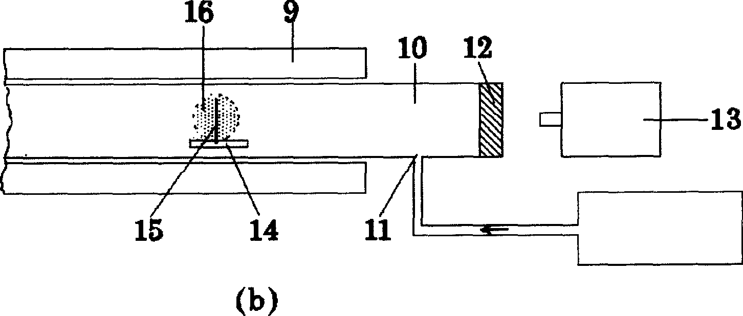
[0017] Embodiment 1: After the alumina ceramic sheet is polished on the surface, it is placed in an ion implanter, and carbon ions of 100 KeV are used for implantation treatment, and the implantation dose is 7×10 18 cm -2 , and then put the injected sample into figure 1 The annealing treatment is performed in the MPCVD equipment shown. Such as figure 1 and figure 2 As shown, the microwave source (marked by the dotted line) is composed of a magnetron 1 with a frequency of 2.45 GHz, an anode ammeter 2, an incident power meter 4, a reflected power meter 5, an air load 6 and a four-screw adjuster 7. The source output power is continuously adjustable, and the maximum power can reach 1000W. The microwave generated by the microwave source has a size of 110×55mm 2 The brass rectangular waveguide 8, the cut-off waveguide 9 and the short-circuit piston 18 are transmitted into the Φ39mm quartz reaction tube 10 in the TE10 mode. The quartz reaction tube 10 is placed horizontally, a...


PUM


Abstract

The present invention relates to microwave plasma chemical vapor deposition process of oriented diamond film on alumina ceramic. The technological process includes the following steps: implanting carbon ion to alumina ceramic before deposition; microwave plasma high-temperature annealing of the alumina ceramic under mixed nitrogen and hydrogen atmosphere; and the oriented deposition of diamond film on the alumina ceramic. During the oriented deposition, the alumina ceramic is set inside the quartz tube reactor with microwave plasma radiation, the reactor is vacuum pumped, inflated with mixed gas of hydrogen and methane, and diamond film of oriented crystal grains is formed through vapor deposition under specific technological condition.

Description

technical field [0001] The invention relates to a method for realizing directional growth of a diamond film on an alumina ceramic substrate, belonging to the field of chemical vapor deposition of inorganic non-metallic materials. Background technique [0002] Alumina ceramics is a packaging substrate material traditionally used in integrated circuits. However, due to the small thermal conductivity of alumina ceramics (~0.2W / cm K), it cannot dissipate the heat of the chip in time, which is not conducive to the development of integrated circuits. The development in the direction of power density; in addition, the dielectric coefficient of alumina ceramics is also large (~10), which will lead to longer signal delay time, thus limiting the development of integrated circuits to higher frequencies. Diamond has the highest thermal conductivity among all substances, and has a low dielectric coefficient, so it is the most ideal packaging substrate and construction substrate material....

Claims


Application Information

Patent Timeline
Patent Type & Authority Applications(China)
IPC IPC(8): C04B41/85C23C16/27C23C16/50
Inventor 夏义本王林军方志军莫要武簧晓琴戴雯琦文黎星张文广
Owner SHANGHAI UNIV
Why Eureka
Try Eureka