Sensor of chip contaonong microelectrode array

A micro-electrode array, chip sensor technology, applied in the direction of instruments, material capacitance, material electrochemical variables, etc., can solve the problems of not using electrochemical detection, the limitation of the object to be analyzed, and the high cost of the chip, and improve the detection sensitivity and film thickness. Uniform, controllable and easy-to-operate effects

Inactive Publication Date: 2003-12-24
FUDAN UNIV
View PDF6 Cites 19 Cited by
  • Summary
  • Abstract
  • Description
  • Claims
  • Application Information

AI Technical Summary

Problems solved by technology

In addition, dozens of patents with application numbers from 01132492 to 01132499, 01135856-01135877, and 01137660-01137677 are all patents related to rice gene chips. None of the methods used electrochemical detection technology
[0005] Existing chips of this type are costly, complicated to operate, and have certain limitations on the objects to be analyzed

Method used


Image

  • Sensor of chip contaonong microelectrode array
  • Sensor of chip contaonong microelectrode array
  • Sensor of chip contaonong microelectrode array

Examples


Embodiment Construction

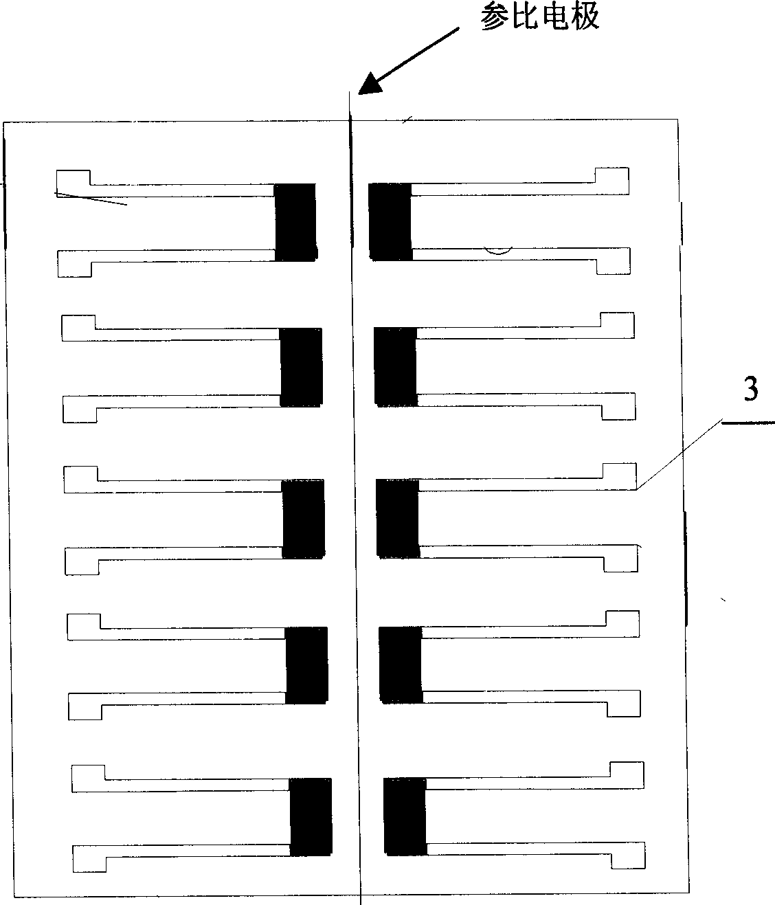
[0032] The base material of the microchip is a piece of n-type or p-type 100 monocrystalline silicon with a size of 3 cm in length and 2.0 cm in width. A layer of metal titanium film with a thickness of 100nm can be prepared on the surface of the silicon chip by vacuum evaporation method by means of physical surface film formation, and then a gold film with a thickness of 300nm can be prepared on it by the same method. The micro-electrode array designed according to needs is made into a negative photomask, and the metal layer (titanium and gold layer) on the part not covered by the mask is removed by photoetching technology. Then, a silicon dioxide insulating layer with a thickness of 150 nm is prepared by using a plasma enhanced chemical deposition method (PECVD, Plasma Enhance Chemical Vapor Deposition) at the position where the metal layer is removed. Then, the entire chip is annealed at a high temperature of 500 degrees for 30 minutes in an oxygen atmosphere. The lead-out...


PUM

PropertyMeasurementUnit
lengthaaaaaaaaaa
widthaaaaaaaaaa
thicknessaaaaaaaaaa

Abstract

A microelectrode array chip sensor on the silicon substrate features that said microelectrode array is composed of interdigital electrodes for smaller gap between positive and negative electrodes andhigher transmission speed of electrons. It is prepared by MEMS technique. Its advantages are simple preparing process and high sensitivity.

Description

technical field [0001] The invention is a micro-electrode array chip sensor based on micro-machining technology. Background technique [0002] Chip sensor is a chemical analysis method that is developing very rapidly in the world. It has many unique advantages, such as high sensitivity, mass production (low price), good dynamic response performance, greatly reduced size, high precision, good reliability, easy to make multi-element sensor arrays, and electronic , chips integrated with mechanical systems, etc. Due to its wide range of applications, it can be used as a variety of chemical and biological sensors, and can work in gas, vacuum and liquid environments. So it can be a real-time and online detection tool for chemical composition biomolecules. These characteristics are difficult to achieve with many other types of sensors. [0003] In the past 10 years, there have been 83 Chinese patents on microarray chips, such as the Chinese patent "Method for preparing compound...

Claims


Application Information

Patent Timeline
Patent Type & Authority Applications(China)
IPC IPC(8): C12Q1/68G01N27/22G01N27/30G01N33/50G01N33/68G01N35/00
Inventor 孔继烈林殷茵刘宝红张松李爱珍黄宜平
Owner FUDAN UNIV
Why Eureka
Try Eureka