Structure of channel shielded Rom memory unit and producing method thereof

A technology of read-only memory and storage unit, which is applied in semiconductor/solid-state device manufacturing, electrical components, electric solid-state devices, etc. It can solve the problems of lateral diffusion of impurities and uneven distribution of ions, reduction of the width of depletion regions, decline of product qualification rate, etc. question

Inactive Publication Date: 2004-02-04
GRACE SEMICON MFG CORP
View PDF0 Cites 4 Cited by
  • Summary
  • Abstract
  • Description
  • Claims
  • Application Information

AI Technical Summary

Problems solved by technology

[0003] The manufacturing process of general shielded read-only memory is basically made by three main steps of deposition (deposition), lithography (photo) and etching (etching) through multiple cycles. The requirements for integration are getting higher and higher, and the design specifications are getting smaller, so that the size of the components is getting smaller and smaller, and the area of ​​ion implantation is also shrinking. In the subsequent thermal process, it is very easy to cause doping The punch through caused by the lateral diffusion of ions makes it impossible to improve the electrical quality of the components, and the product qualification rate decreases.
[0004] On the other hand, although the size of the device is reduced, the width of the depletion layer caused by the uneven distribution of ions between adjacent bit lines cannot be reduced due to the reduction of the device size. , an unresolved problem
[0005] In the traditional method of manufacturing high-density shielded read-only memory, the area of ​​the memory cell is reduced and the distance between two adjacent bit lines is reduced in the face of higher and higher integration of components, which makes the lateral diffusion of impurities and ions The problem of depleted areas caused by uneven distribution is more significant, which will make it difficult to manufacture smaller shielded ROMs, and reduce the yield and electrical quality of components

Method used


Image

  • Structure of channel shielded Rom memory unit and producing method thereof
  • Structure of channel shielded Rom memory unit and producing method thereof
  • Structure of channel shielded Rom memory unit and producing method thereof

Examples


Embodiment Construction

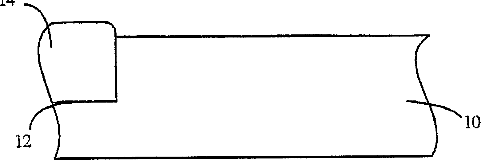
[0011] see Figure 1A Firstly, a silicon substrate 10 is provided, and a shallow trench isolation structure is formed in the silicon substrate 10, and a shallow trench isolation (shallow trench isolation, STI) process is used to form a shallow trench isolation (STI) process on the silicon substrate by using lithography and etching processes. A shallow trench isolation 12 is formed in 10, and then a shallow trench isolation oxide (STI oxide) 14 is formed to fill the shallow trench isolation 12 by chemical vapor deposition (CVD) process.

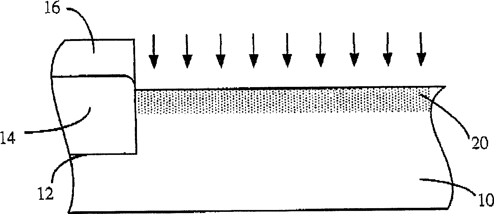
[0012] see again Figure 1B , forming a patterned photoresist 16 on the silicon substrate 10 by lithography etching to cover the shallow trench isolation oxide layer 14, and performing an ion implantation step, the ion implantation step is to simultaneously perform a buried ion doping impurity and breakdown-resistant ion doping, wherein the buried-type ion doping is to implant buried N-type (buried N+) ions into the silicon substrate 10, and ...


PUM


Abstract

In the method, a shallow ditch is formed on surface of a silicon base material and to implant simultaneously buried ion and anti-punch through dopand in the silicon base material and array region of internal memory storage unit. The buried ion doping region is defined and multiditch is formed at array region of the storage unit. Then, a gate-oxide and a patternized polysilicon grid are formed at the silicon base material and furthermore multitransistor can be formed at peripheral circuit region of the silicon base material.

Description

【Technical field】 [0001] The present invention relates to the structure of a semiconductor component and its manufacturing method, in particular to a shielded read-only memory (mask read-only memory, Mask ROM) in which multiple trenches are formed in the memory storage unit array area of ​​a silicon substrate with its method of manufacture. 【Background technique】 [0002] The basic structure of the shielded ROM is that a plurality of word lines and bit lines are arranged in an interlaced manner, and each word line and each bit line are parallel and electrically insulated from each other, and one word line and one bit line are mutually parallel and electrically insulated. The gate and the surrounding space formed by the intersection of the lines form the storage unit of the shielded read-only memory, and whether any storage unit is turned on or not is determined by the adjustment of the initial voltage of the storage unit in the encoding program. Decision, to achieve the pur...

Claims


Application Information

Patent Timeline
Patent Type & Authority Applications(China)
IPC IPC(8): H01L21/8246H01L27/112
Inventor 张有志叶双凤
Owner GRACE SEMICON MFG CORP
Why Eureka
Try Eureka