Joint tool for supersonic wave joint

A bonding tool, ultrasonic technology, applied in the direction of semiconductor devices, electrical components, circuits, etc., can solve problems such as insufficient hardness, damage to tool surface shape accuracy, and wear

Inactive Publication Date: 2004-02-25
SUMITOMO ELECTRIC IND LTD
View PDF1 Cites 5 Cited by
  • Summary
  • Abstract
  • Description
  • Claims
  • Application Information

AI Technical Summary

Problems solved by technology

[0005] Metal tools that have been used in the past have insufficient hardness on the front end surface of the tool, so when mounting, due to broken semiconductor elements and fragments of substrate materials (Si, etc.), and chips attached when cutting elements, etc. There is a problem that the shape accuracy of the tool surface is impaired due to defects formed on the surface of the tool surface, or wear caused by sliding with the semiconductor element, and the life of the bonding tool is shortened.
[0006] In addition, the bonding strength of semiconductor elements is closely related to the applied ultrasonic intensity. The stronger the ultrasonic intensity, the stronger the bonding strength. However, if the ultrasonic intensity is too high, there will be a problem that the position of the element will shift due to ultrasonic vibration.

Method used


Image

  • Joint tool for supersonic wave joint
  • Joint tool for supersonic wave joint
  • Joint tool for supersonic wave joint

Examples


Embodiment 1

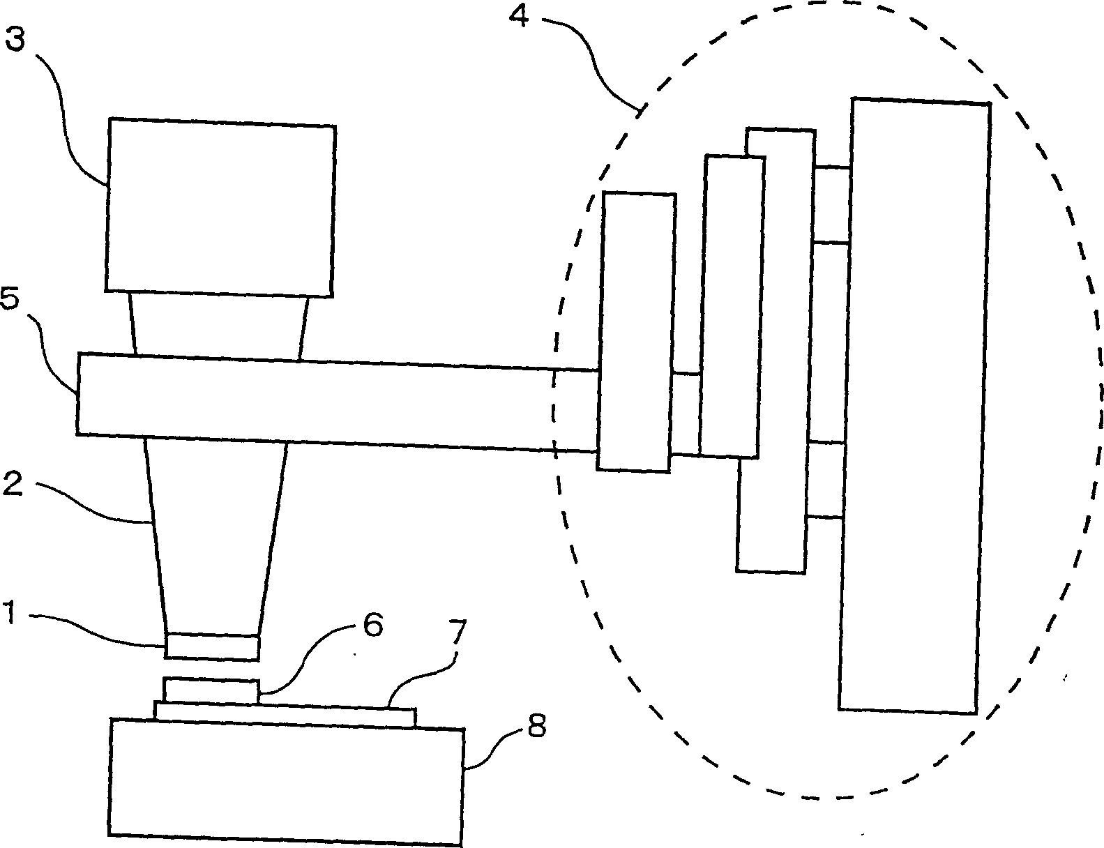
[0024]Sintered diamond, ceramic formed body coated with vapor phase synthetic diamond and cubic boron nitride sintered body are used as the material of the tool tip to make a bonding tool with ultrasonic waves. After the tool tip is formed into a necessary shape, the surface roughness of the tool surface is adjusted. If the surface roughness Rt of the tool face is less than 0.2 μm, the surface of the tool face should be ground, and if the Rt is greater than 0.2 μm but less than 5 μm, the surface of the tool face should be finished by surface grinding. If the Rt is more than 5 μm, after surface grinding of the surface of the tool face, laser processing is used to roughen the surface. As the horn part, FeNiCo alloy, nickel-iron-molybdenum permeable alloy, superhard alloy, stainless steel and cermet can be processed into the shape of ultrasonic horn respectively.

[0025] In a vacuum furnace, the front end of the tool and the horn are metal-bonded with an active brazing filler m...

Embodiment 2

[0031] FeNiCo alloys, nickel-iron-molybdenum permeable alloys, superhard alloys and cermets are used to make the horns of ultrasonic bonding tools, and the front faces of these horns are coated with diamond films by vapor phase synthesis. As the vapor phase synthesis method, a hot-filament CVD (chemical vapor deposition) method is used.

[0032] The synthesis condition of the hot wire CVD (chemical vapor deposition) method is to make the flow rate H of the gas raw material 2 10-100 sccm, CH 4 1-5 sccm, the filament temperature is 1500-2200°C, the substrate temperature is 500-900°C, the pressure is 10-500 Torr, and the synthesis time is changed according to the necessary film thickness. After the diamond film is coated, the diamond film is thick, and the flatness and surface roughness of the diamond surface cannot meet the required precision. Therefore, it is necessary to grind and grind it into the necessary shape with a diamond grindstone. In addition, for comparison, a hor...

Embodiment 3

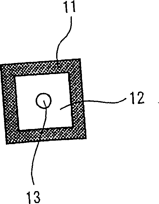
[0037] Five types of tools were manufactured by laser processing by partially changing the roughness of the front end surface of the bonding tool produced in the same manner as in Example 1 1-1, and bonding of 5000 semiconductor elements was carried out in the same manner as in Example 1. The bonding tool was produced so that the surface roughness of the outer peripheral portion of the tool tip surface was greater than that of the central portion, and the ratio of the overall area of ​​the tool tip surface to the portion with a large surface roughness was varied. A tool not provided with a rough surface was also produced as a comparative example, and the same mounting evaluation was performed. figure 2 It is a plan view schematically showing the tool front end surface of the produced bonding tool. The results of bonding are shown in Table 3.

[0038] Ratio of Roughness

detailed status

3-1

10%

Displacement of substrate electrodes and elemen...


PUM

PropertyMeasurementUnit
hardnessaaaaaaaaaa
particle sizeaaaaaaaaaa
thicknessaaaaaaaaaa

Abstract

PURPOSE: To provide a bonding tool for ultrasonic bonding with which an electrode of a semiconductor element is efficiently and stably bonded to an electrode of a substrate by a flip-chip basis in a process of mounting the semiconductor element on the substrate by using mainly ultrasonic energy. CONSTITUTION: A material which has high hardness and good heat conductivity is applied to a tool tip to be brought into contact with the semiconductor element to realize both a long life and high-level bonding. Further, the surface roughness of the surface of the tool tip is adjusted to efficiently propagate the ultrasonic energy and also prevent the element from shifting in position.

Description

technical field [0001] The present invention relates to a bonding tool used when applying ultrasonic energy to a semiconductor element by flip-chip method to bond it to an electrode of a substrate in semiconductor manufacturing technology. Background technique [0002] The flip-chip mounting method is a mounting method in which electrode terminals (bumps) for two-dimensional input and output are arranged on the back of a semiconductor element, and the bumps are directly metal-bonded to electrode terminals on the substrate side. Because this method can connect multiple input and output terminals in a short distance, the installation area is small, so it is suitable for high-density installation of high-speed operating components, and the number of installations can be increased dramatically by this method. [0003] In this flip-chip method, as one of methods for mounting a semiconductor element on a substrate, a method of performing bonding by diffusion bonding of interface a...

Claims


Application Information

Patent Timeline
Patent Type & Authority Applications(China)
IPC IPC(8): H01L21/60H01L21/449H01L21/607
CPCH01L24/75H01L2924/10253H01L2224/75312H01L2224/75353H01L2924/00H01L21/607
Inventor 山本佳津子藤冈昭文中井哲男石桥惠二关裕一郎
Owner SUMITOMO ELECTRIC IND LTD
Why Eureka
Try Eureka