Producing method for shallow ridges separation

A manufacturing method and shallow trench technology, applied in semiconductor/solid-state device manufacturing, electrical components, circuits, etc., to solve problems affecting component performance, etc.

Inactive Publication Date: 2004-09-22
SILICON INTEGRATED SYSTEMS
View PDF0 Cites 11 Cited by
  • Summary
  • Abstract
  • Description
  • Claims
  • Application Information

AI Technical Summary

Problems solved by technology

Therefore, if the thickness of the silicon nitride layer 103 varies between wafers (wafer to wafer) or on the same wafer (within wafer), the siz

Method used


Image

  • Producing method for shallow ridges separation
  • Producing method for shallow ridges separation
  • Producing method for shallow ridges separation

Examples


Embodiment Construction

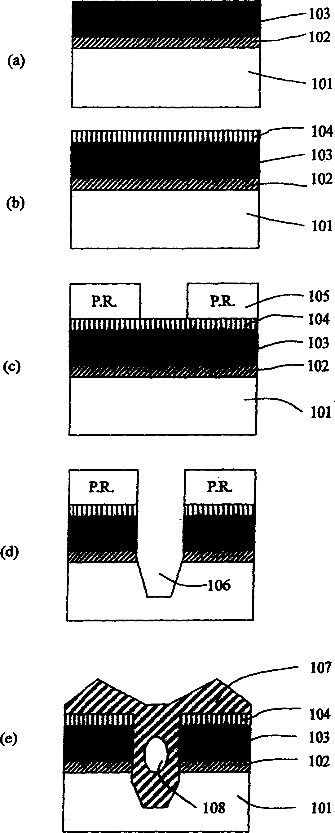
[0025] Please refer to Figure 4 . Figure 4 It is a cross-sectional view of the manufacturing process of the first embodiment of the present invention. Figure 4 (a) shows that a pad oxide layer 102 is grown on a silicon substrate 101 by a dry oxidation method, and its thickness is about 50 Å to 200 Å to reduce defects on the silicon surface and relieve the stress of the subsequently deposited silicon nitride layer 103 , and then deposit a layer of silicon nitride layer 103 on the pad oxide layer 102 by LPCVD or PECVD, with a thickness of about 500 Å to 2000 Å, as a hard mask when etching shallow trenches.

[0026] refer to Figure 4 (b), Figure 4 (b) shows that a silicon oxynitride layer 401 with a high absorption coefficient is deposited on the silicon nitride layer 103 first, and then a silicon oxynitride layer 402 with a low absorption coefficient is deposited as an anti-reflection layer. A method of depositing a silicon oxynitride layer with a high absorption coeffi...


PUM


Abstract

The present invention discloses a manufacturing method of the shallow isolating trough. In this method some SiON layers with a specific thickness and the different absorptive coefficients are deposited on a silicon nitride film, which comprises the following steps: ( a ) depositing a silicon oxide / silicon nitride pad film as an etching mask on a silicon substrate; (b) depositing a SiON layer with the high absorption coefficient on the silicon nitride layer first and then a SiON layer with the low absorption coefficient as an anti-reflective layer; (c) performing the photolithography with a photomask of the shallow trough and developing the exposed photoresist to form the etching mask of the shallow trough; (d) etching the SiON, the silicon nitride, the silicon oxide pad layer and the silicon substrate to form the shallow trough; (e) growing a silicon oxide layer on the side wall and bottom of the shallow trough to remove the damage and reduce the electric leakage; (f) depositing a silicon oxide layer in the shallow trough and on the SiON to fill up the trough; (g) flatting the surface by abrading chemically and mechanically.

Description

technical field [0001] The invention relates to a manufacturing method for shallow trench isolation of semiconductor integrated circuits. In particular, it relates to a method of depositing SiON reflective layers with different absorption coefficients to reduce the influence of silicon nitride film thickness on exposure, and to control the width of the STI opening to control the size of the active region and improve the trench filling performance of the STI. Background technique [0002] Integrated circuit manufacturing technology is rapidly developing towards miniaturization along with Moore's Law, and the chip size is continuously shrinking due to the improvement of integration level to increase the number of components per unit area of ​​the chip. The line width (critical dimension, CD) used in the production line has entered the field of nano-miter (nm) from sub-micron (Sub-micron), and most of the exposure light sources used use wavelengths of 248nm or even 193nm to imp...

Claims


Application Information

Patent Timeline
IPC IPC(8): H01L21/76
Inventor 林平伟郭国权姜兆声
Owner SILICON INTEGRATED SYSTEMS
Why Eureka
Try Eureka