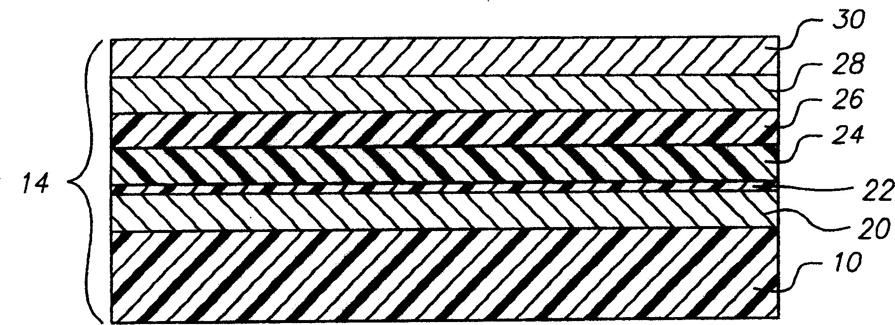
Forming improved stabiity emissive layer from donor element in OLED device
A technology of stability and emission layer, applied in electrical components, electric solid-state devices, semiconductor devices, etc., can solve problems such as lowering stability, and achieve the effect of lowering working voltage, improving stability, and improving working stability
- Summary
- Abstract
- Description
- Claims
- Application Information
AI Technical Summary
Problems solved by technology
Method used
Image

Examples
Embodiment 1
[0134] Embodiment 1 (the embodiment of the present invention)
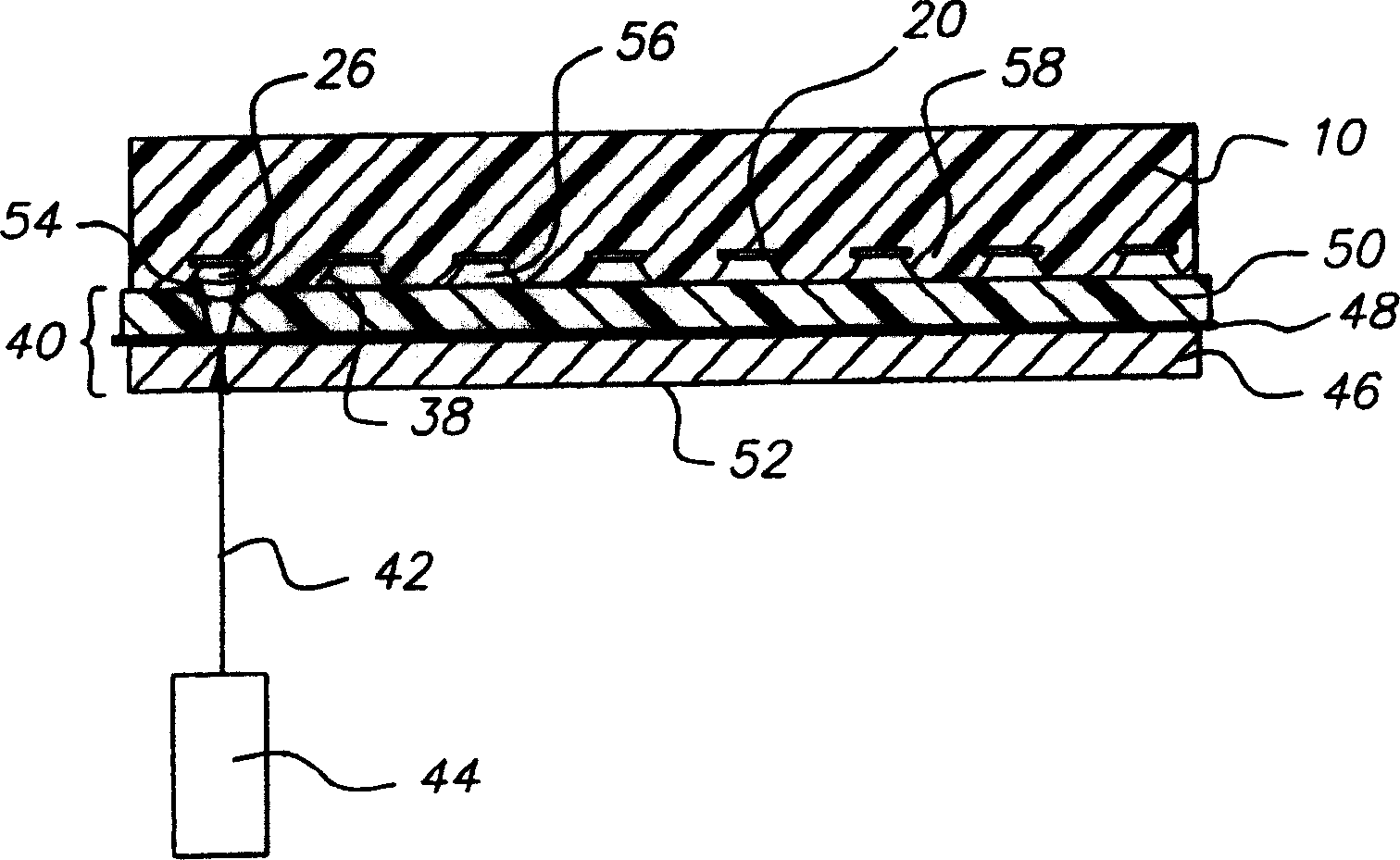
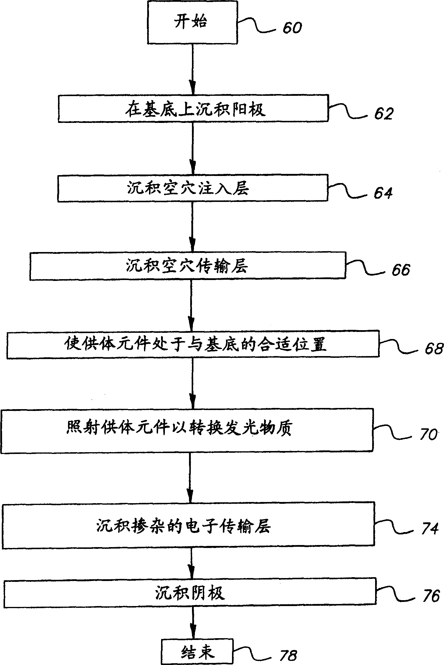
[0135] An OLED device meeting the requirements of the present invention and doped with an organic layer of a low work function metal is manufactured by the following method:
[0136] 1. Vacuum deposition of indium tin oxide (ITO) on a clean glass substrate to form a 34nm thick transparent electrode.
[0137] 2. The ITO surface prepared above was treated with plasma oxygen etching, followed by plasma deposition of a 1.0 nm layer of fluorocarbon polymer (CFx) as described in US-A-6,208,075.
[0138] 3. At about 10 -6 The substrate prepared above was further processed by vacuum deposition under Torr vacuum to deposit 170 nm 4,4'-bis[N-(1-naphthyl)-N-phenylamino]biphenyl (NPB ) hole transport layer.
[0139] 4. The substrate prepared above was removed from the vacuum and exposed to air for about 5 minutes before being placed in a nitrogen oven.
[0140] 5. Prepare a donor substrate by vacuum coating 40 nm of chr...
Embodiment 2
[0149] Embodiment 2 (comparative example)
[0150] OLED devices were fabricated using the method described in Example 1, except for step 11 (depositing an electron transport layer) as follows:
[0151] 11. A 35 nm electron transport layer of tris(8-quinolinate)aluminum(III) (ALQ) was vacuum deposited on the substrate with a coating station including a heated boat source.
[0152] result
[0153] Example
[0154] The device without doped low work function metal organic layer (Example 2) has significantly shorter half-life and higher voltage than the device with doped low work function metal organic layer (Example 1). Adding a lithium dopant to the electron transport layer increases the half-life by more than 2 times (Example 2 compared to Example 1), thus improving the stability of the device.
PUM
 Abstract
Description
Claims
Application Information
 - R&D
- Intellectual Property
- Life Sciences
- Materials
- Tech Scout
- Unparalleled Data Quality
- Higher Quality Content
- 60% Fewer Hallucinations
Browse by: Latest US Patents, China's latest patents, Technical Efficacy Thesaurus, Application Domain, Technology Topic, Popular Technical Reports.
© 2025 PatSnap. All rights reserved.Legal|Privacy policy|Modern Slavery Act Transparency Statement|Sitemap|About US| Contact US: help@patsnap.com