

Plasma etching method and plasma treatment apparatus
A plasma and etching device technology, which is applied in the field of plasma technology, can solve the problems of low plasma density distribution uniformity and etching uniformity, unable to obtain etching rate, and RF power increase, etc., and achieves good etching ability and etching. The effect of increased rate, improved uniformity
- Summary
- Abstract
- Description
- Claims
- Application Information
AI Technical Summary
Problems solved by technology
Method used
Image

Examples
Embodiment 1
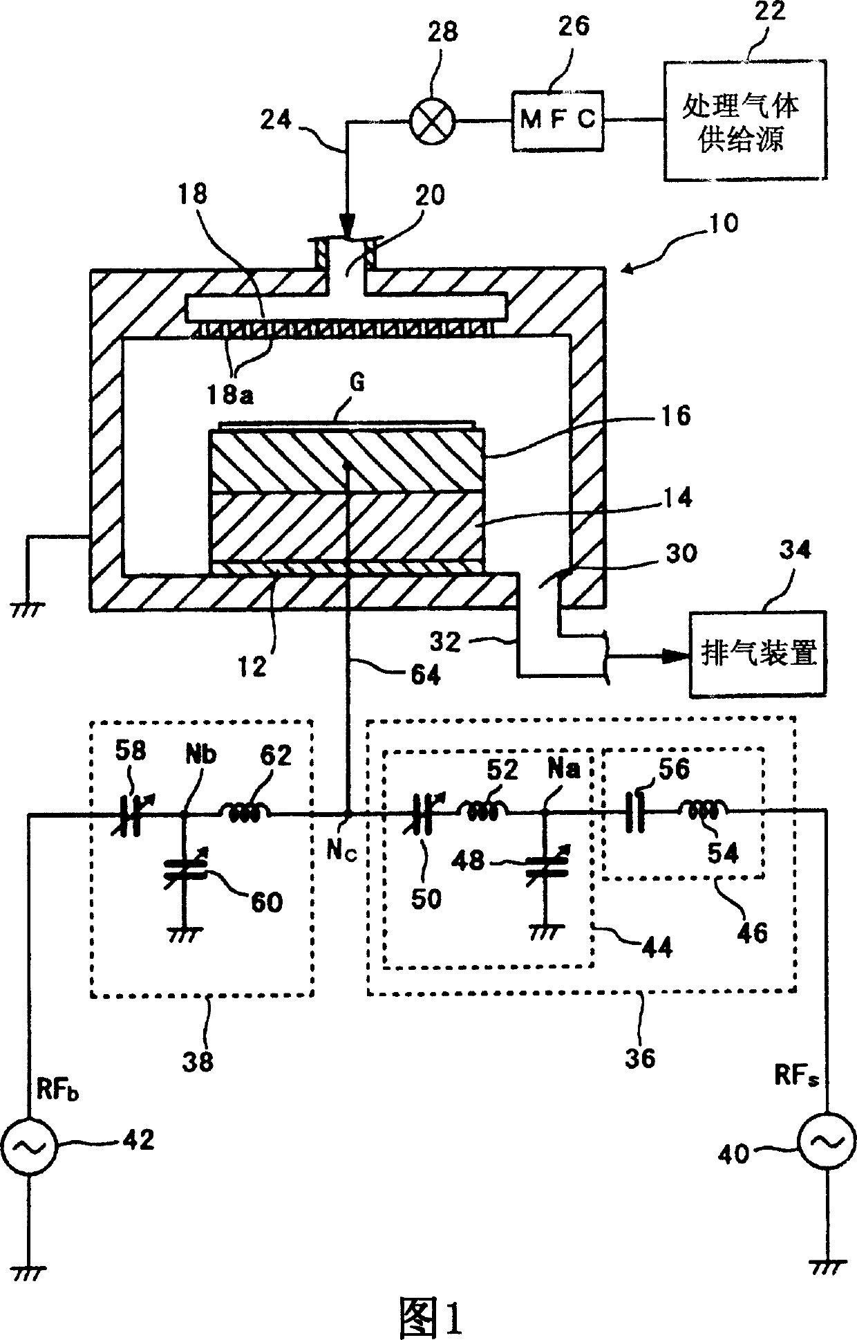
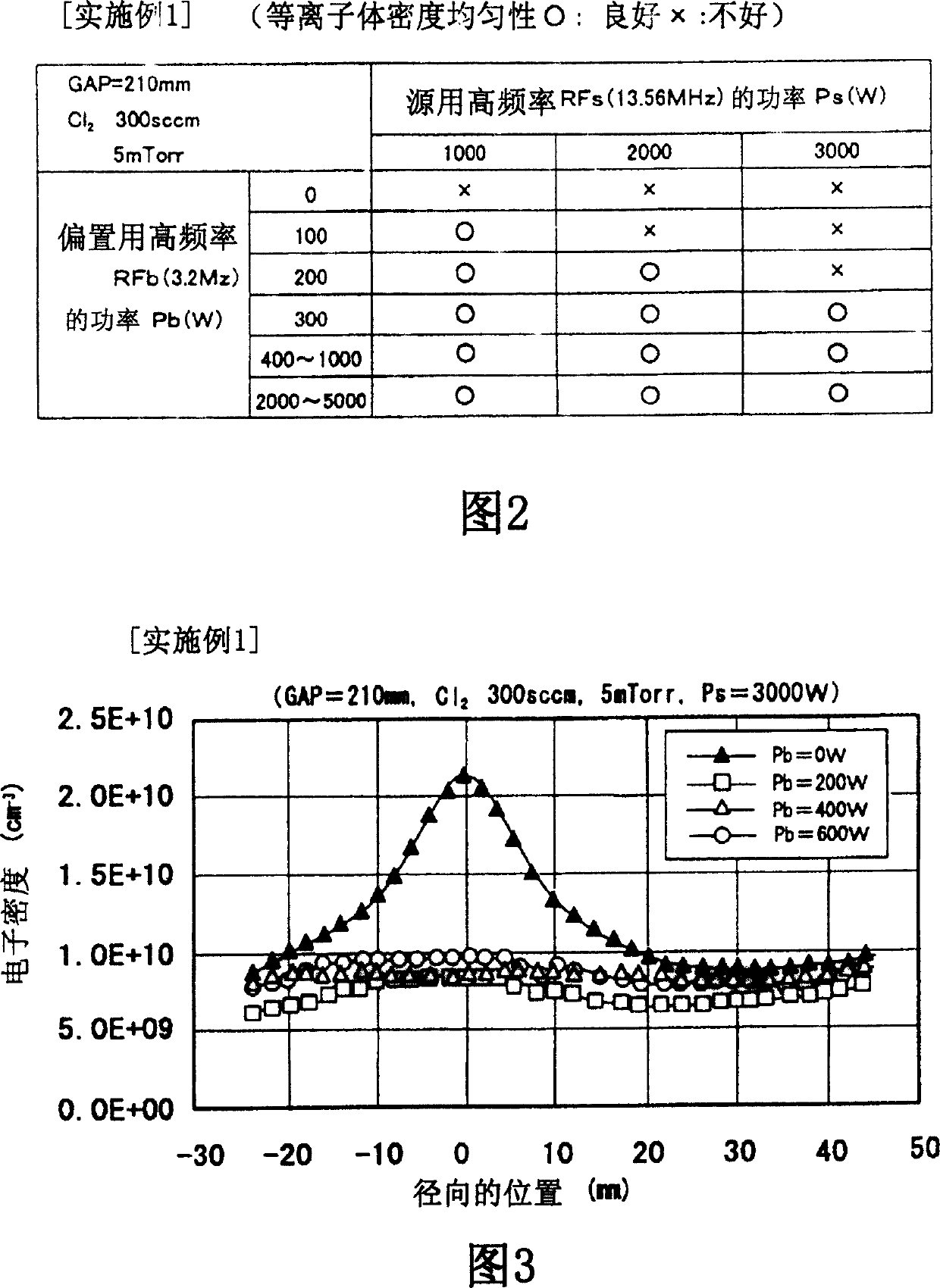
[0050] Using the plasma etching apparatus of Fig. 1, the source in the etching of aluminum (Al) is used with high-frequency RF s (13.56MHz) power Ps and high frequency RF for bias b (3.2 MHz) power Pb was used as a parameter to evaluate the uniformity of the plasma density distribution.
[0051]In a multilayer wiring structure in which aluminum wiring is provided, it is desirable to perform tapered etching on the lower layer, especially on the aluminum wiring on the lowermost layer, in order to facilitate embedding of the insulating film. In the aluminum and tapered etching of FPD, in order to achieve anisotropic etching, it is desired to reduce the pressure and increase the high-frequency RF for the source s The power of Ps.
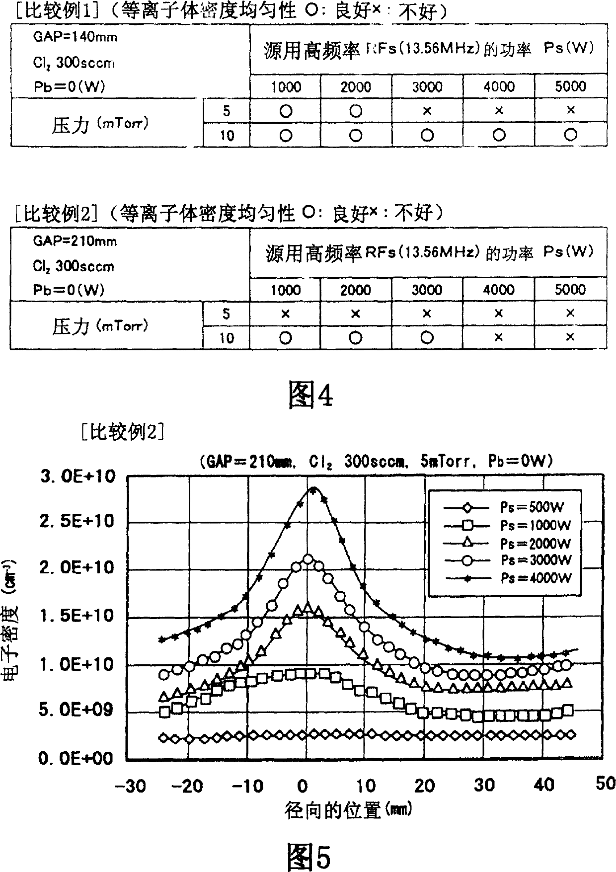
[0052] However, as shown in Comparative Examples 1, 2, and 3 in Fig. 4 to Fig. b while using only the source with high frequency RF s In the single-frequency application method, the higher the RF s The lower the pressure in the chamber, the lower t...
Embodiment 2
[0057] Using the plasma etching apparatus shown in Fig. 1, in the etching of aluminum neodymium (AlNd), which is a kind of aluminum alloy, high-frequency RF b (3.2MHz) power Pb is used as a parameter to evaluate the size of the etching rate. As other main etching conditions, the gap between electrodes (GAP) is set at 140 mm, chlorine gas Cl 2 (Flow rate 300sccm) as etching gas, the pressure in the chamber is set at 5mTorr, the temperature (upper electrode (T) / lower electrode (B) / chamber side wall (W)) = 60 / 20 / 60°C, the source uses high Frequency RF s (13.56MHz) power Pb was set at 2000W. Can use BCl 3 and other halogen gases as etching gases.
PUM
 Abstract
Description
Claims
Application Information