Method for preparing high quality ZnO single crystal thin film on (La, Sr) (Al, Ta) O3

A single-crystal thin-film, high-quality technology, used in semiconductor/solid-state device manufacturing, electrical components, circuits, etc., to solve problems such as large film strain, poor crystal quality and optoelectronic properties, and lattice mismatch.

Inactive Publication Date: 2005-03-02
INST OF PHYSICS - CHINESE ACAD OF SCI
View PDF0 Cites 11 Cited by
  • Summary
  • Abstract
  • Description
  • Claims
  • Application Information

AI Technical Summary

Problems solved by technology

However, the in-plane orientation relationship between the ZnO epitaxial film grown along the c-axis and the LSAT(111) substrate prepared by the existing method is often inconsistent with the above ideal situation, and the in-plane epitaxial orientation is ZnO‖ LSAT and ZnO‖LSAT, there

Method used


Image

  • Method for preparing high quality ZnO single crystal thin film on (La, Sr) (Al, Ta) O3
  • Method for preparing high quality ZnO single crystal thin film on (La, Sr) (Al, Ta) O3
  • Method for preparing high quality ZnO single crystal thin film on (La, Sr) (Al, Ta) O3

Examples


Embodiment Construction

[0019] The present invention will be described in detail below in conjunction with the preparation method of the present invention and the accompanying drawings.

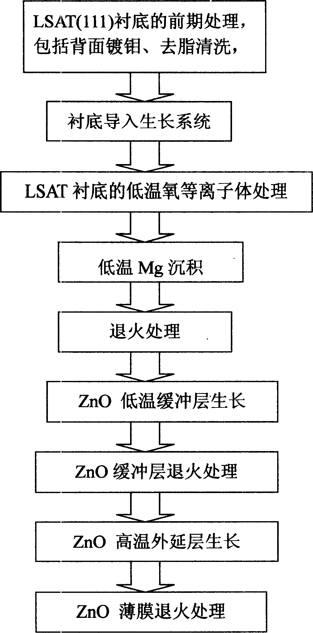
[0020] Such as figure 1 Shown process flow diagram of the present invention, the concrete steps of preparing high-quality O polarity ZnO single crystal thin film on LSAT (111) substrate are as follows:

[0021] 1) Plating molybdenum on the back of the LSAT (111) substrate, degreasing and cleaning, and then introducing the substrate into the molecular beam epitaxy growth system;

[0022] 2) Perform radio frequency oxygen plasma treatment at a low temperature of 180° C. for 30 minutes, the radio frequency power is 350 W, and the oxygen flow rate is 2.5 sccm to obtain an LSAT (111) substrate with an O-terminated surface;

[0023] 3) At air pressure -7 When the Pa and the substrate temperature are 180°C to deposit metallic magnesium, the equivalent vapor pressure of the magnesium beam is 1×10 -5 Pa, control the deposi...


PUM


Abstract

The prodn. steps are: 1) to do low-temp. oxygen plasma preprocessing to LSAT(111) substrate surface, 2) to deposit magnesium ultrathin layer in ultrahigh vacuum and low temp., 3) to do annealing process to magnesium ultrathin layer by increasing substrate temp. to make magnesium atoms moving and deabsorbing on LSAT (111) substrate, 4) to obtain ultrathin magnesium adsorption layer, thus to realize that ZnO film grows according to crystal lattice small mismatch and epitaxial orientation to produce atom grade smooth high-quality ZnOfilm with single O polarity and domain. The smooth ZnO film produced by the invention has high crystal quality and photoelectric performance.

Description

technical field [0001] The invention relates to a method for preparing a wide bandgap semiconductor zinc oxide (ZnO) single crystal film, especially in (La, Sr) (Al, Ta) O 3 (LSAT for short) (111) A method for obtaining high-quality ZnO single crystal thin films by controlling epitaxial orientation, eliminating spin domains, and controlling polarity when preparing zinc oxide thin films on substrates. Background technique [0002] ZnO has a variety of superior properties and is widely used in transparent conductive films, surface acoustic wave devices and piezoelectric ceramics. ZnO is also a direct transition II-VI semiconductor with a band gap of 3.37eV at room temperature. Due to its high free exciton binding energy (60meV), ZnO has become another important wide-bandgap semiconductor material after GaN, and has a very broad application prospect in the preparation of low-threshold, high-efficiency short-wavelength optoelectronic devices. The preparation of device-quality ...

Claims


Application Information

Patent Timeline
IPC IPC(8): H01L21/365
Inventor 杜小龙薛其坤英敏菊梅增霞曾兆权郑浩
Owner INST OF PHYSICS - CHINESE ACAD OF SCI
Why Eureka
Try Eureka